Thin film structure for high density inductors and redistribution in wafer level packaging
a technology of inductors and thin films, applied in semiconductor devices, semiconductor/solid-state device details, electrical devices, etc., can solve the problems of pvd circuitry being limited to 10-20 micron lines and spaces, and achieving circuit lines of high resolution below 10 microns is more difficult, so as to promote adhesion and promote long-term reliability of wafer level packaging , the effect of high density
- Summary
- Abstract
- Description
- Claims
- Application Information
AI Technical Summary
Benefits of technology
Problems solved by technology
Method used
Image

Examples
Embodiment Construction
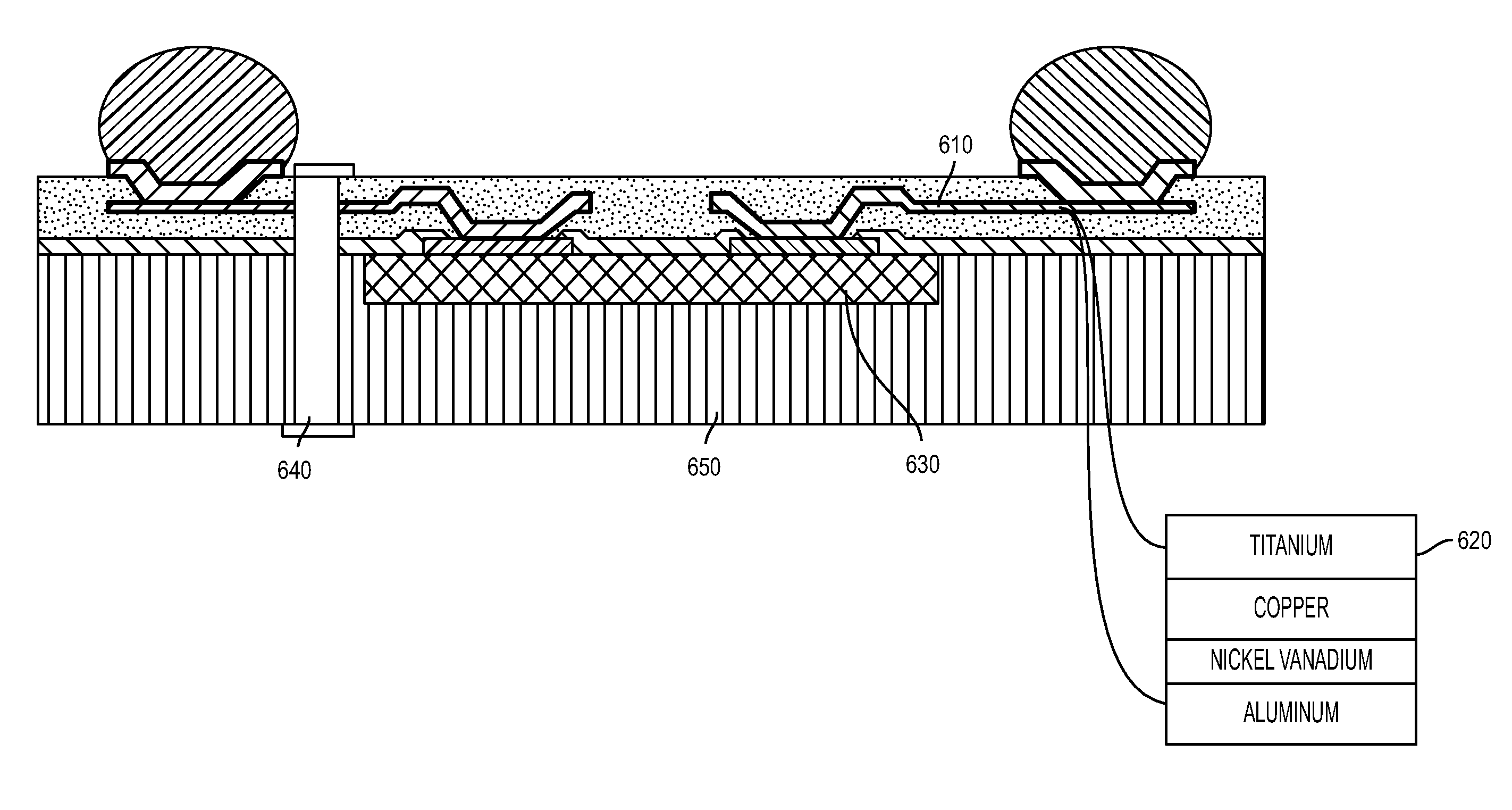
[0020]One or more embodiments of the present disclosure are directed to an improved, reliable and manufacturable method of achieving high yields on additive circuitry with the faster and thinner PVD process for wafer level packaging. In one or more embodiments, the improved method provides a means to significantly simplify the manufacturing flow and reduce the cost of manufacturing by the use of a titanium thin film adhesion layer on the metal stack comprising the seed layer. This titanium film remains with the circuitry in the final product and typically has a thickness of about 250 angstroms, but can have various thicknesses depending on the application.
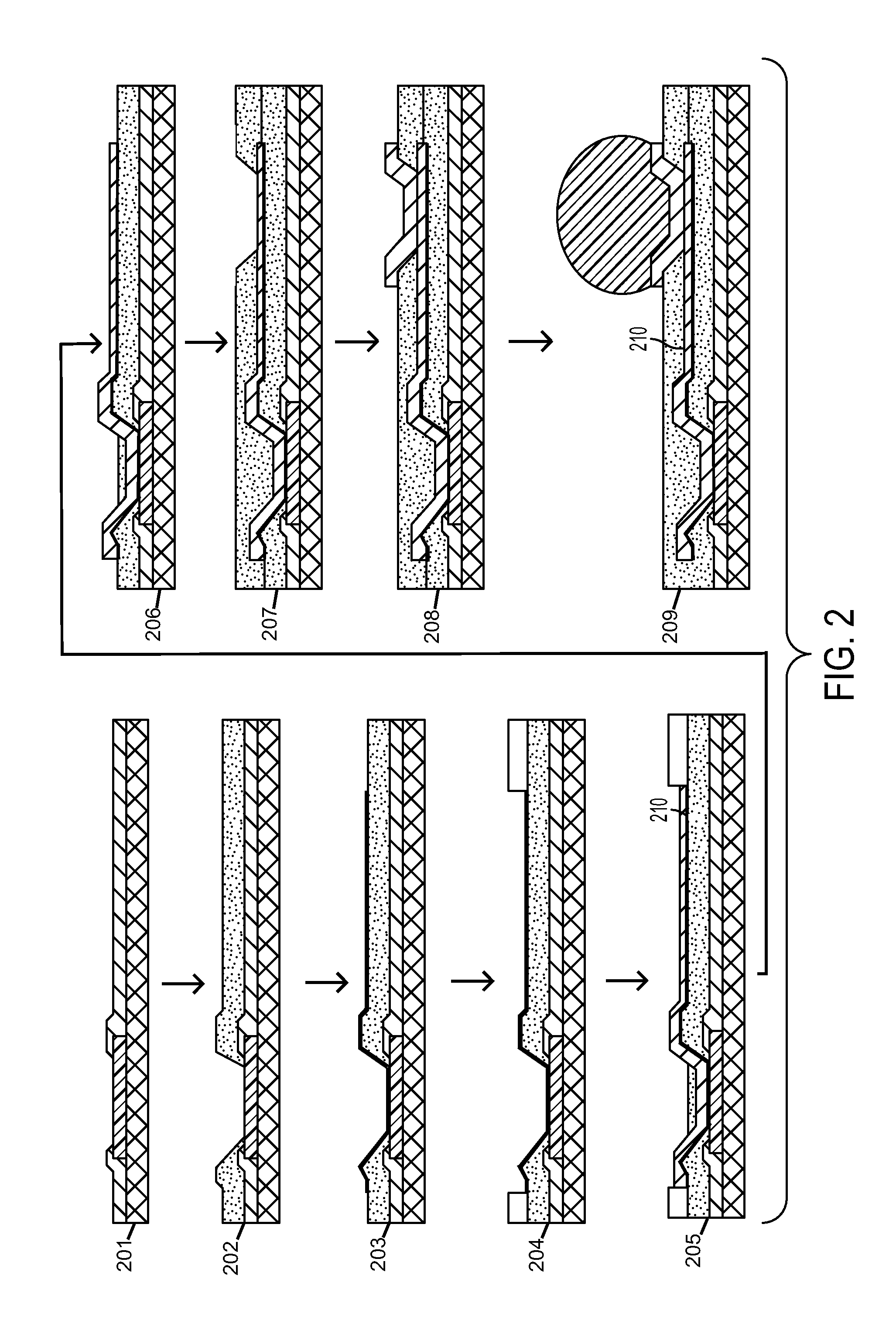
[0021]Referring now to FIG. 4, in an embodiment, a process for forming an RDL circuitry runner 410 with a titanium enabled metal stack structure 420 in accordance with one or more embodiments of the present disclosure is disclosed. The process illustrated by the structure 401 includes the operations of coating the first dielectric ...
PUM
| Property | Measurement | Unit |
|---|---|---|
| thickness | aaaaa | aaaaa |
| thickness | aaaaa | aaaaa |
| thickness | aaaaa | aaaaa |
Abstract
Description
Claims
Application Information
 - R&D Engineer
- R&D Manager
- IP Professional
- Industry Leading Data Capabilities
- Powerful AI technology
- Patent DNA Extraction
Browse by: Latest US Patents, China's latest patents, Technical Efficacy Thesaurus, Application Domain, Technology Topic.
© 2024 PatSnap. All rights reserved.Legal|Privacy policy|Modern Slavery Act Transparency Statement|Sitemap