Unlock instant, AI-driven research and patent intelligence for your innovation.

Output buffers

a buffer and output technology, applied in the field of output buffers, can solve the problems of gate oxide breakdown, mos transistor damage, and high voltage level damage, and achieve the effect of high voltage toleran

Active Publication Date: 2015-04-28
VIA TECH INC
View PDF5 Cites 0 Cited by
  • Summary
  • Abstract
  • Description
  • Claims
  • Application Information

AI Technical Summary

Benefits of technology

[0005]It is desirable to provide an output buffer with high voltage tolerance, which can prevent MOS transistors of the output buffer from being damaged by external signals with high voltage levels.
[0006]An exemplary embodiment of an output buffer is provided. The output buffer is coupled to a first voltage source providing by a first supply voltage and used for generating an output signal at an output terminal according to input signal. The output buffer comprises a first transistor, a second transistor, and a self-bias circuit. The first transistor has a control electrode, an input electrode coupled to the output terminal, and an output electrode. The second transistor has a control electrode, an input electrode coupled to the output electrode of the first transistor, and an output electrode coupled to a reference voltage. The self-bias circuit is coupled to the output terminal and the control electrode of the first transistor. When the output buffer does not receive the first supply voltage, the self-bias circuit provides a first bias voltage at the control electrode of the first transistor according to the output signal to decrease voltage differences between the control electrode and the input and output electrodes of the first transistor to be lower than a predetermined voltage.
[0007]Another exemplary embodiment of an output buffer is provided. The output buffer is coupled to a first voltage source providing a first supply voltage and used for generating an output signal at an output terminal according to an input signal. The output buffer comprises a first transistor, a second transistor, a first diode, a third transistor, and a fourth transistor. The first transistor has a control electrode, an input electrode coupled to the first voltage source, and an output electrode. The second transistor has a control electrode, an input electrode coupled to the output electrode of the first transistor, and an output electrode. The first diode has an anode coupled to the output electrode of the second transistor and a cathode coupled to the output terminal. The third transistor has a control electrode, an input electrode coupled to the output terminal, and an output electrode. The fourth transistor has a control electrode, an input electrode coupled to the output electrode of the third transistor, and an output electrode coupled to a reference voltage. The self-bias circuit is coupled to the output terminal and the control electrode of the third transistor. When the output buffer does not receive the first supply voltage, the self-bias circuit provides a first bias voltage at the control electrode of the first transistor according to the output signal to decrease voltage differences between the control electrode and the input and output electrodes of the third transistor to be lower than a predetermined voltage. The control electrodes of the first transistor and the second transistor are controlled according to the input signal.

Problems solved by technology

High voltage devices cannot be manufactured by the advanced CMOS processes.
When the MOS transistors fabricated with the 28 nm processes receive these signals, the MOS transistors may be damaged by the high voltage levels.
For example, high voltage differences between the gate and source / drain of the MOS transistors (i.e. large Vgs or Vgd) may result in gate oxide breakdown, and high voltage differences between the source and drain of the MOS transistors (i.e. large Vds) may result in punch-through.

Method used


Image

  • Output buffers
  • Output buffers
  • Output buffers

Examples


Embodiment Construction

[0014]The following description is made for the purpose of illustrating the general principles of the invention and should not be taken in a limiting sense. The scope of the invention is best determined by reference to the appended claims.

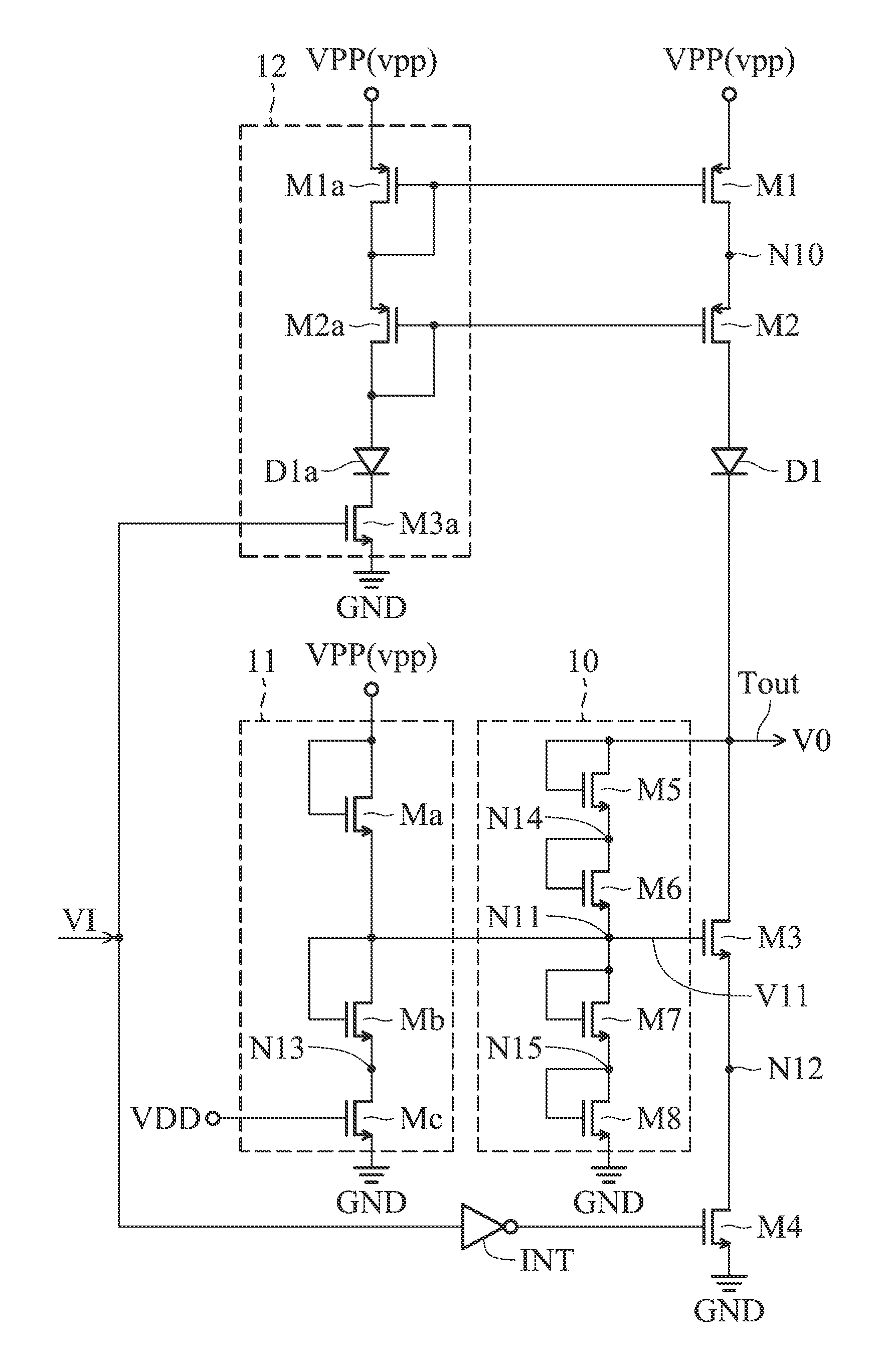
[0015]In a large electronic system having multiple sub-systems, such as in a computer system, there are generally multiple power levels. The sub-systems, such as integrated circuits (ICs) and chips in the system often require different power voltages. Therefore, to protect the subsystems from being damaged by the different power voltages, an input / output buffer circuit is generally provided between the sub-systems. In a system having a first circuit on a first chip, a second circuit on a second chip, and an input / output buffer circuit coupled in between, the power supply of the first circuit (denoted as VDD) may have a lower voltage level than that of the second circuit (denoted as VPP). For example, the first circuit may operate at a power level (...


PUM


Abstract

An output buffer is provided. The output buffer is coupled to a first voltage source providing a first supply voltage and used for generating an output signal at an output terminal according to an input signal. The output buffer includes first and second transistors and a self-bias circuit. The first and second transistors are cascaded between the output terminal and a reference voltage. The self-bias circuit is coupled to the output terminal and the control electrode of the first transistor. When the output buffer does not receive the first supply voltage, the self-bias circuit provides a first bias voltage to the control electrode of the first transistor according to the output signal to decrease voltage differences between the control electrode and the input and output electrodes of the first transistor to be lower than a predetermined voltage.

Description

BACKGROUND OF THE INVENTION[0001]1. Field of the Invention[0002]The invention relates to an output buffer, and more particularly, to an output buffer with high voltage tolerance.[0003]2. Description of the Related Art[0004]Nowadays, in advanced CMOS (Complementary Metal-Oxide-Semiconductor) processes (such as 28 nm processes), the gate oxide breakdown voltage and drain-source punch-through voltage of MOS transistors are lower as compared with previous processes (such as 40 nm processes). High voltage devices cannot be manufactured by the advanced CMOS processes. For example, 3.3V devices may not be manufactured by the 28 nm processes. However, some peripheral components or other ICs not manufactured by advanced processes may still operate in high voltages such as 3.3V. The signals generated in the peripheral components or other ICs may have high voltage levels. When the MOS transistors fabricated with the 28 nm processes receive these signals, the MOS transistors may be damaged by t...

Claims


Application Information

Patent Timeline
Patent Type & Authority Patents(United States)
IPC IPC(8): H03K3/00G05F3/24
CPCG05F3/24
Inventor LEE, YEONG-SHENG
Owner VIA TECH INC