Transient liquid phase bonding process for double sided power modules

a technology of transient liquid phase and power electronics, which is applied in the direction of manufacturing tools, non-electric welding apparatus, soldering apparatus, etc., can solve the problems of complicated assembly process, increased manufacturing costs, and increased manufacturing costs, so as to reduce the dependence of thickness limitation, fast and reliable fabrication, and reduce the effect of excessive bonding tim

Active Publication Date: 2015-06-02
DENSO CORP
View PDF129 Cites 1 Cited by
  • Summary
  • Abstract
  • Description
  • Claims
  • Application Information

AI Technical Summary

Benefits of technology

[0008]TLP enables fast and reliable fabrication of a substantially homogeneous bondline with reduced dependency of a thickness limitation. Stated another way, a substantially homogeneous bondline made of substantially a single alloy without a thickness limitation and excessive bonding time can be achieved using the techniques disclosed herein. A (more) suitable bondline providing better and targeted performance for power electronics may also be achieved. Because the resulting bond has a re-melting temperature (i.e., a sustainable temperature) significantly larger than its bonding temperature, TLP may be particularly useful for high temperature power electronic devices, such as electronic devices fabricated from silicon, SiC, GaN, etc. For example, TLP bonding is at least applicable to automotive (including hybrid, plug-in hybrid, and / or electrical vehicles), watercraft, aerospace, nuclear, and / or electronics industries. TLP bonding is highly adaptable and is at least applicable to wafer-to-wafer, die-to-wafer, die-to-substrate, or die-to-die bonding. Moreover, this system is compatible with conventional fabrication techniques and can be adapted for use in double-sided bonding.

Problems solved by technology

Because multiple devices need to be aligned and bonded, simultaneous bonding requires a complex assembly process.
For instance, when placing the power device and the top and bottom components in a fixture for soldering, the top component and the power device may obscure the view of the bottom component, which complicates checking the alignment.
Solder reflow may further create misalignment.

Method used


Image

  • Transient liquid phase bonding process for double sided power modules
  • Transient liquid phase bonding process for double sided power modules
  • Transient liquid phase bonding process for double sided power modules

Examples


Embodiment Construction

[0021]In the following detailed description, numerous specific details are set forth to provide an understanding of the present invention. It will be apparent, however, to one ordinarily skilled in the art that elements of the present invention may be practiced without some of these specific details. In other instances, well-known structures and techniques have not been shown in detail to avoid unnecessarily obscuring the present invention.

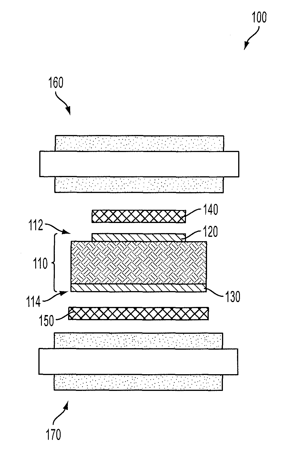
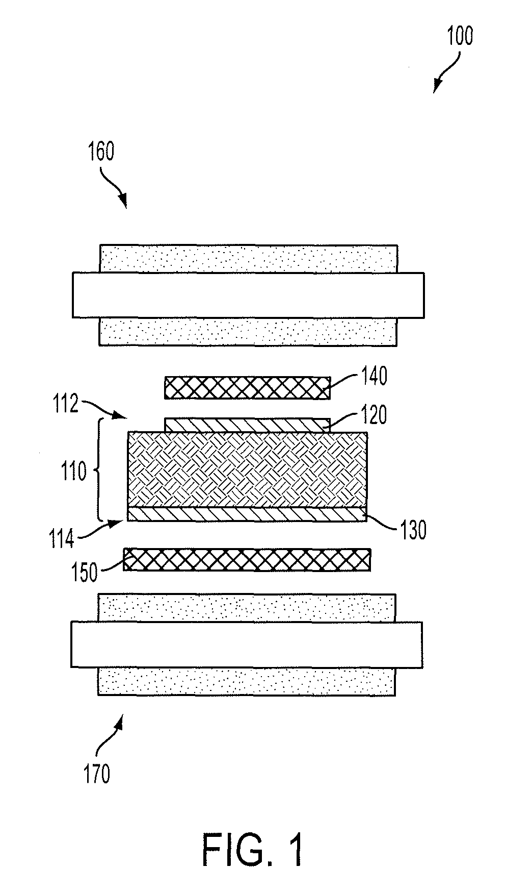
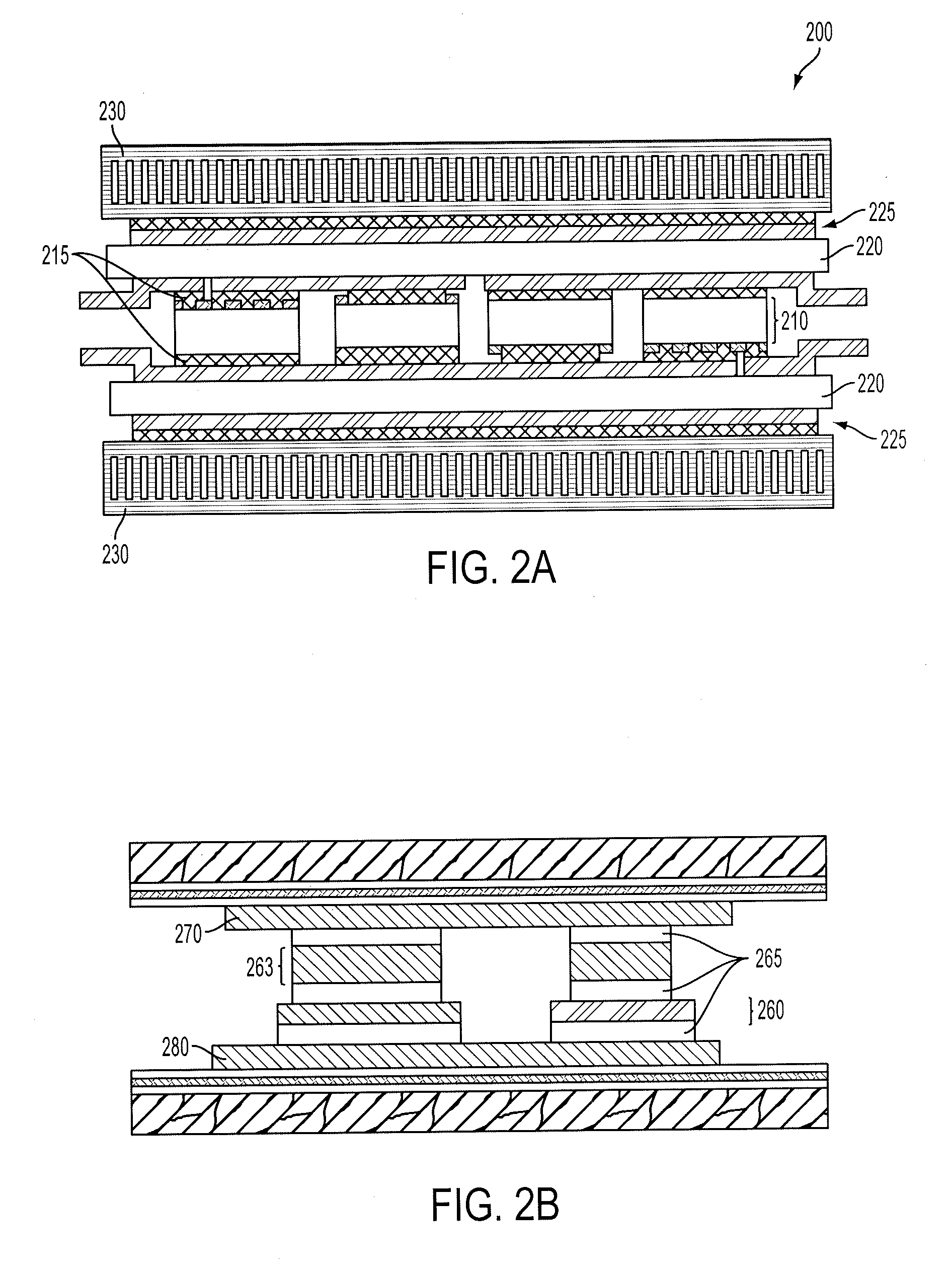
[0022]The present invention is generally directed to an improved bonding via transient liquid phase bonding in power electronics. Transient liquid phase (TLP) bonding produces joints that have microstructural and hence mechanical properties different to those properties of the base materials. TLP bonding differs from solder bonding in which diffusion occurs when a melting point depressant element from an interlayer moves into lattice and grain boundaries of the substrates at the bonding temperature. Solid state diffusional processes lead to a chan...


PUM

PropertyMeasurementUnit
melting pointaaaaaaaaaa
temperatureaaaaaaaaaa
thermalaaaaaaaaaa

Abstract

A double-sided bonding process using transient liquid phase (TLP) bonding structure. A first side of an electronic device is processed to partially complete bonding. A second side of the electronic device is processed to complete bonding. The first side completes bonding during the processing of the second side. This reduces the time needed for the bonding process of both sides. This process allows for various TLP bonding parameters while being compatible with conventional fabrication systems.

Description

CROSS REFERENCE TO RELATED APPLICATIONS[0001]This application claims the benefit and priority of U.S. Provisional Application No. 61 / 843,296, filed on Jul. 5, 2013, which is hereby incorporated by reference in its entirety. This application incorporates by reference the entire contents of U.S. patent application Ser. No. 13 / 448,632, filed on Apr. 17, 2012.BACKGROUND[0002]1. Field[0003]The present invention relates to alloy formation, and more particularly, to double-sided bonding using transient liquid phase (TLP) bonding in power electronics.[0004]2. Description of the Related Art[0005]Double-sided bonding of power devices and other electrical devices allows for power module structures having improved thermal and electrical performance by attaching components to both the top and bottom sides of an electronic device. For example, double-sided bonding allows for double-sided cooling or chip-on-chip designs. Solder, either lead or lead-free, is commonly used for double-sided bonding.[...

Claims


Application Information

Patent Timeline
Patent Type & Authority Patents(United States)
IPC IPC(8): B23K31/02B23K20/00B23K1/00B23K20/02H05K13/00
CPCB23K20/02H05K13/0023B23K1/0016B23K2201/36B23K20/026B23K20/16B23K20/22H01L24/83H01L2924/1305H01L2924/13055H01L2924/13091H01L24/33H01L2224/83101B23K2101/42H01L24/29H01L24/32H01L2224/2908H01L2224/32502H01L2224/04026H01L2224/29026H01L2224/29083H01L2224/29139H01L2224/29144H01L2224/29147H01L2224/32225H01L2224/33181H01L2224/83815H01L2224/8382H01L2224/29155H01L2224/2612H01L2924/00H01L2924/00014H01L2924/0105H01L2924/014H01L2924/01049B23K2101/36H05K13/00
Inventor YOON, SANG WONKATO, TAKEHIROSHIOZAKI, KOJI
Owner DENSO CORP
Why Eureka
Try Eureka