Flash memory cell with capacitive coupling between a metal floating gate and a metal control gate

a capacitive coupling and flash memory technology, applied in the field of logic process type flash memory, can solve the problems of limited logic process, add cost to logic chips, and difficulty in scaling eflash memory cells, etc., and achieve the effects of reducing the programming voltage of logic based flash memory cells, enhancing capacitive coupling, and high resistan

Active Publication Date: 2015-06-02
QUALCOMM INC
View PDF20 Cites 3 Cited by
  • Summary
  • Abstract
  • Description
  • Claims
  • Application Information

AI Technical Summary

Benefits of technology

[0005]Systems and methods of manufacturing a logic based flash memory cell (e.g., an embedded electrical erasable flash memory cell) without adding extra masks and process steps are disclosed. The described techniques may enable a logic based flash memory cell (e.g., the flash memory cell is implemented using logic gates) to be manufactured by using a high-k / metal gate manufacturing process (e.g., in a sub-28 nm manufacturing process) to enhance capacitive coupling between a floating gate and a control gate of a logic based flash memory cell. The use of high-k / metal gate with a high resistance metal plate manufacturing process enables tuning of the capacitive coupling between the floating gate and the metal control gate; thus, a programming voltage of the logic based flash memory cell may be reduced as compared to the use of a gate oxide diode coupling device. Improving coupling efficiency and reducing programming voltage may reduce design complexity and power consumption of a logic based flash memory cell.
[0007]The flash MTP memory cell may be implemented as a flash memory cell circuit. In a particular embodiment, the flash memory cell circuit is implemented using p-type transistors. The flash memory cell circuit may include a storage transistor and an access transistor. The storage transistor may be serially coupled to the access transistor. A gate of the storage transistor may be coupled to a first plate of a plate capacitor. The first plate may correspond to the floating gate and a second plate of the plate capacitor may correspond to the control gate. The use of the plate capacitor may simplify design complexity of the memory cell as the plate capacitor may be biased to either a positive voltage or to a negative voltage instead of limiting a bias voltage to only a positive voltage or only a negative voltage. When combined with a substrate well and source line or bit line voltage, the use of the plate capacitor may reduce voltage of control gate, source line voltage or bit line voltage while keeping a program voltage or an erase voltage sufficient for a program operation and / or an erase operation.
[0010]One particular advantage provided by at least one of the disclosed embodiments is an ability to manufacture a logic based flash memory cell using a high-k / metal gate manufacturing process. The use of a high-k / metal gate manufacturing process enables tuning of capacitive coupling between a floating gate and a metal control gate of the logic based flash memory cell; thus, a programming voltage of the logic based flash memory cell may be reduced as compared to the use of a gate oxide diode coupling between the floating gate and the control gate. Improving coupling efficiency and reducing programming voltage may reduce design complexity and power consumption of a logic based flash memory cell. Other aspects, advantages, and features of the present disclosure will become apparent after review of the entire application, including the following sections: Brief Description of the Drawings. Detailed Description, and the Claims.

Problems solved by technology

Implementing eflash memory cells may add cost to a logic chip due to the use of additional masks (4˜12 masks) and process, scaling of a eflash memory cell may be difficult due to flash memory cell physical limitations and logic process constraints.
Logic based eflash multi-time programmable (MTP) device may have no process cost adder but may be limited by logic process.
For example, scaling of a logic based (e.g., implemented using logic gates) low density eflash memory cell that involves a single polysilicon layer and gate oxide thickness with limited charge loss due to data retention and without increased cost becomes more challenging as the logic based eflash memory cell moves below 65 nanometer (nm) technology.
For example, a logic based eflash memory cell having a single polysilicon layer and thinner gate oxide that is manufactured using a 45 nm process may not reliably store electrical charge.
The logic based eflash memory cell may have inadequate program and erase performance due to gate oxide capacitive diode coupling between the floating gate and the coupling gate.
The diode coupling limits bias type for program and erase and causes additional charge loss.

Method used


Image

  • Flash memory cell with capacitive coupling between a metal floating gate and a metal control gate
  • Flash memory cell with capacitive coupling between a metal floating gate and a metal control gate
  • Flash memory cell with capacitive coupling between a metal floating gate and a metal control gate

Examples


Embodiment Construction

, and the Claims.

IV. BRIEF DESCRIPTION OF THE DRAWINGS

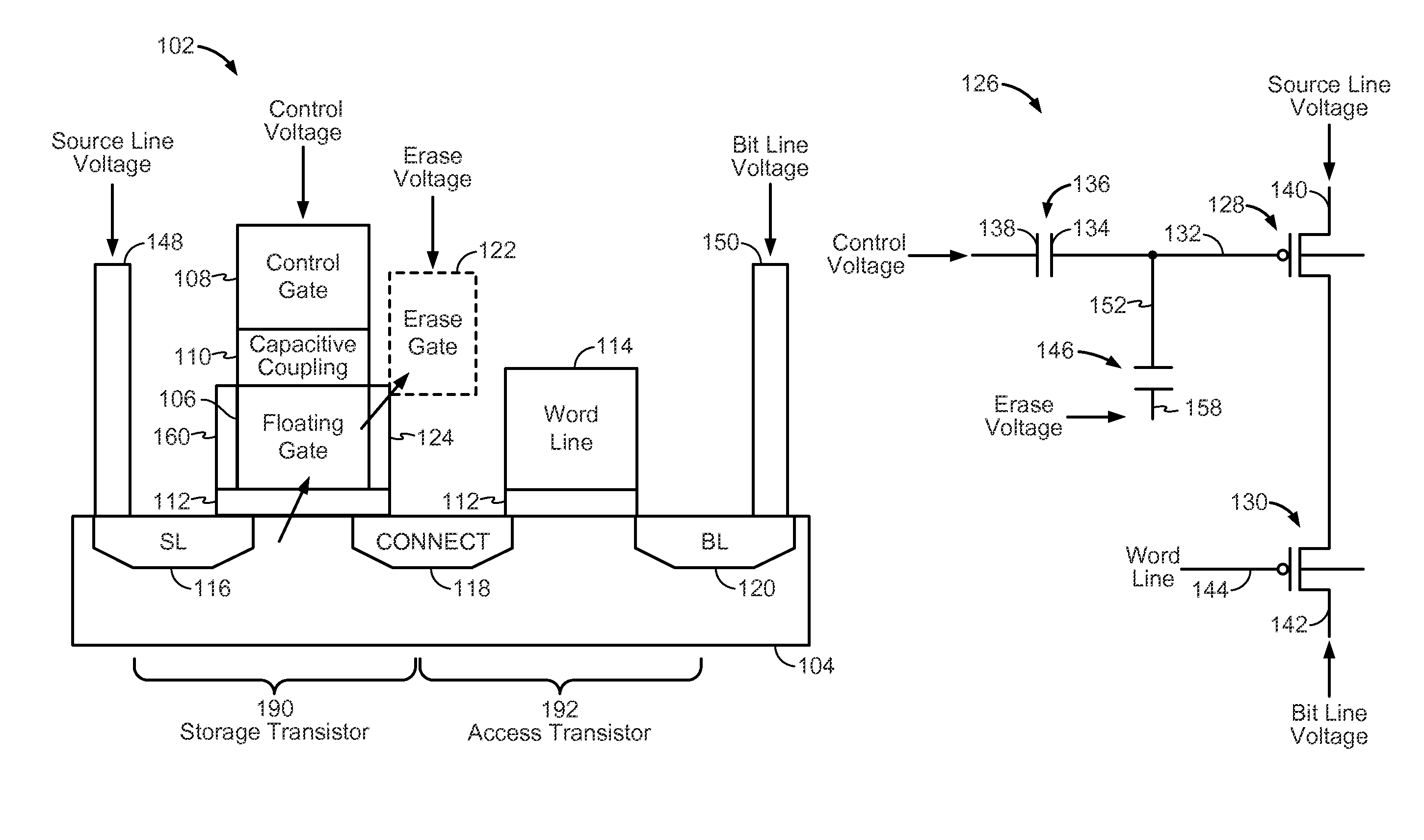
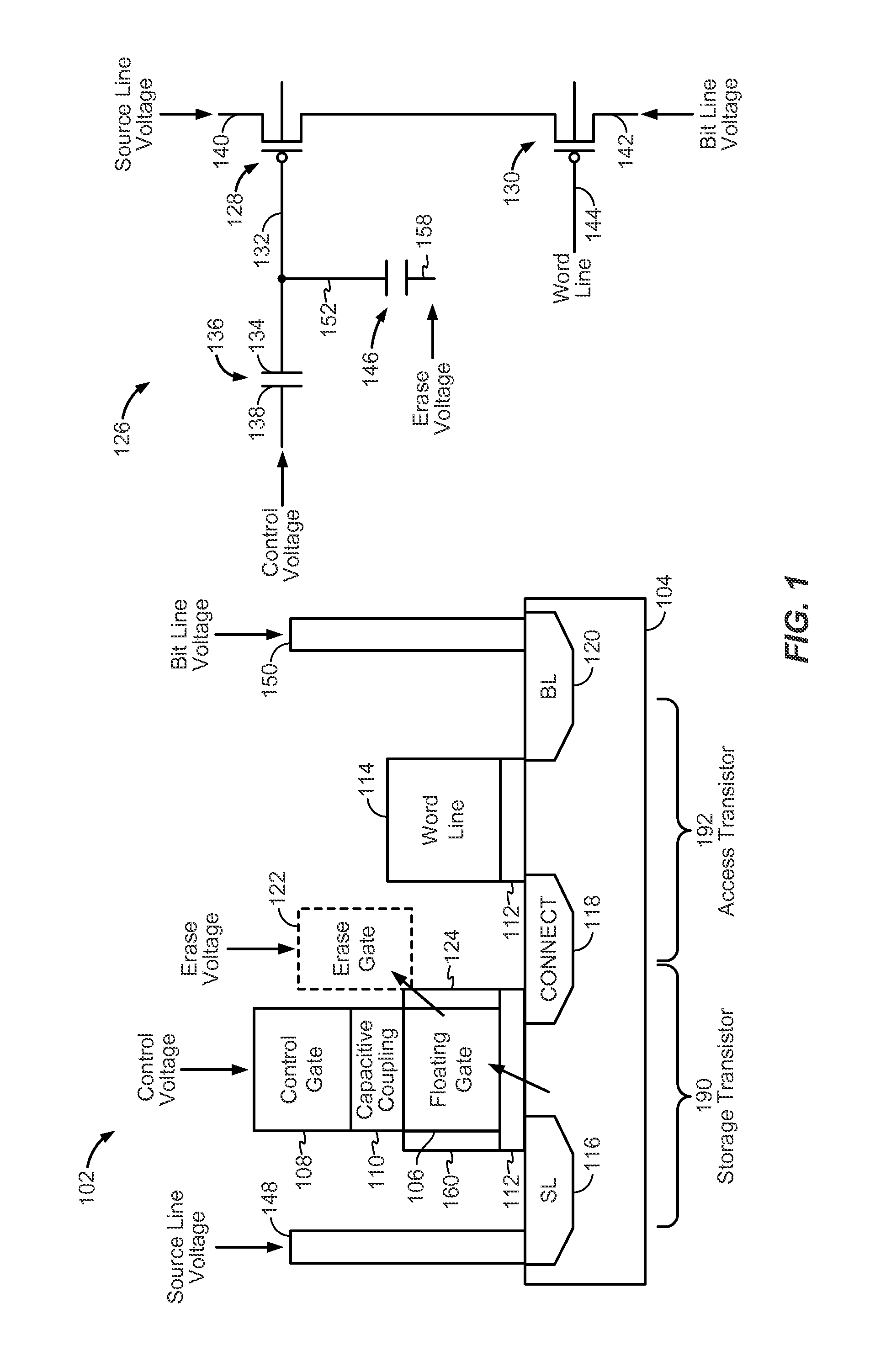
[0011]FIG. 1 is a diagram of a particular embodiment of a flash memory cell that is manufactured using a high-k / metal gate manufacturing process;

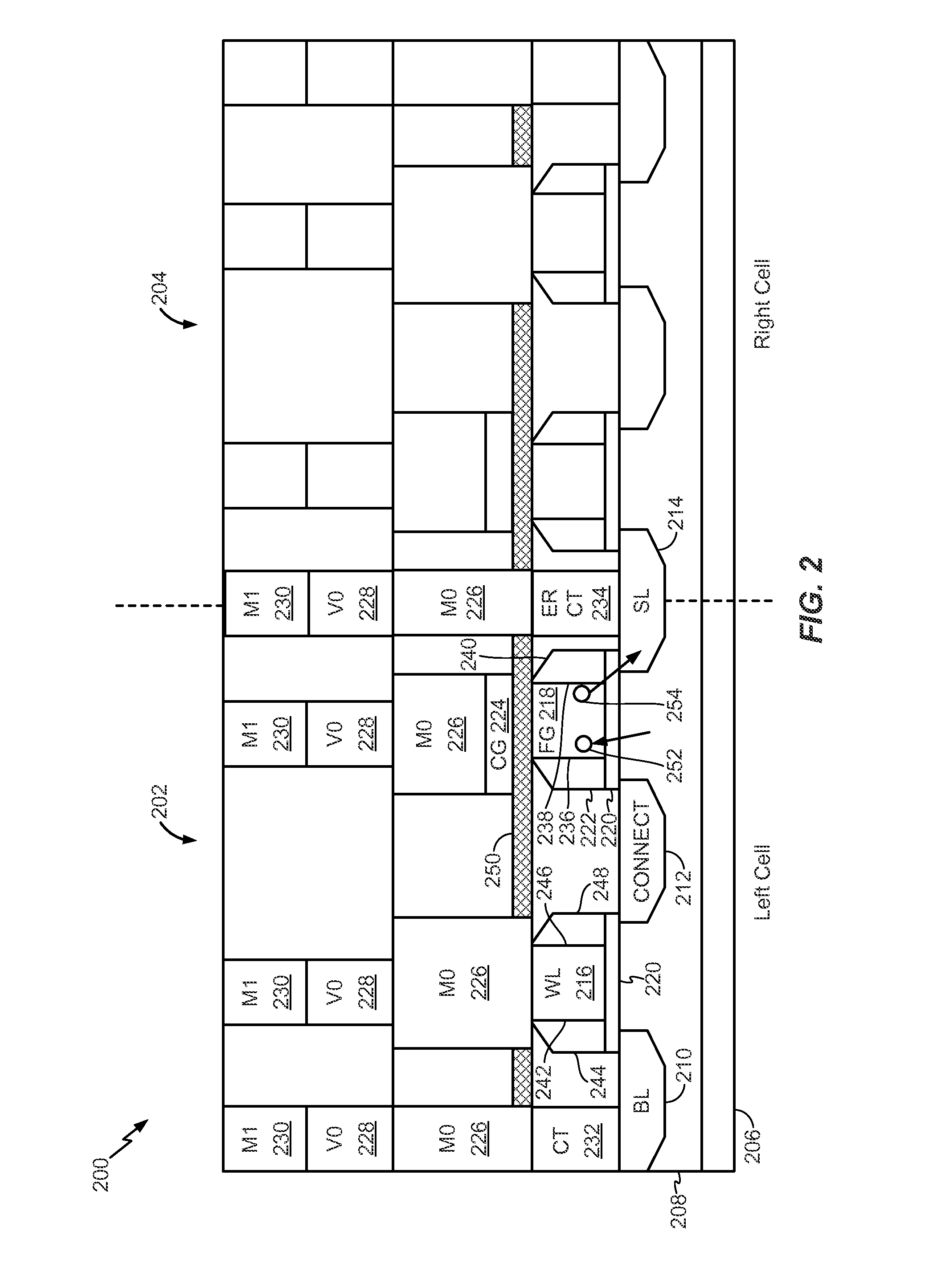
[0012]FIG. 2 is a cross section view of a particular embodiment of a flash memory cell array that includes a flash memory cell manufactured using a high-k / metal gate manufacturing process;

[0013]FIG. 3 is a cross section view of another particular embodiment of a flash memory cell array that includes a flash memory cell manufactured using a high-k / metal gate manufacturing process;

[0014]FIG. 4 is a cross section view of another particular embodiment of a flash memory cell array that includes a flash memory cell manufactured using a high-k / metal gate manufacturing process;

[0015]FIG. 5 is a cross section view of another particular embodiment of a flash memory cell array that includes a flash memory cell manufactured using a high-k / metal gate manufacturing process;

[0016]FIG. 6 is a cross sect...


PUM


Abstract

An apparatus includes a storage transistor. The storage transistor includes a floating gate configured to store electrical charge and a control gate. The floating gate is coupled to the control gate via capacitive coupling. The floating gate and the control gate are metal. The apparatus also includes an access transistor coupled to the storage transistor. A gate of the access transistor is coupled to a word line. The storage transistor and the access transistor are serially coupled between a bit line and a source line.

Description

I. FIELD[0001]The present disclosure is generally related to logic process type flash memory.II. DESCRIPTION OF RELATED ART[0002]Advances in technology have resulted in smaller and more powerful computing devices. For example, there currently exist a variety of portable personal computing devices, including wireless computing devices, such as portable wireless telephones, tablet computers, and paging devices that are small, lightweight, and easily carried by users. More specifically, portable wireless telephones, such as cellular telephones and internet protocol (IP) telephones, can communicate voice and data packets over wireless networks. Further, many such wireless telephones include other types of devices that are incorporated therein. For example, a wireless telephone can also include a digital still camera, a digital video camera, a digital recorder, and an audio file player. Also, such wireless telephones can process executable instructions, including software applications, s...

Claims


Application Information

Patent Timeline
Patent Type & Authority Patents(United States)
IPC IPC(8): G11C16/00G11C16/10G11C16/14H01L21/28H01L29/66
CPCG11C16/10H01L21/28273H01L29/66825G11C16/14G11C16/0433H01L29/42328H01L29/7881H01L29/40114H10B41/30
Inventor LI, XIAYANG, BINWANG, ZHONGZE
Owner QUALCOMM INC
Why Eureka
Try Eureka