Non-volatile memory circuit

a memory circuit and non-volatile technology, applied in static storage, digital storage, instruments, etc., can solve the problems of increasing the area and the number of processes, the memory capacity of the bleeder resistor trimming is small, and the structure of the element becomes complicated, so as to improve the write characteristics and improve the write characteristics

Inactive Publication Date: 2015-06-09
ABLIC INC
View PDF5 Cites 0 Cited by
  • Summary
  • Abstract
  • Description
  • Claims
  • Application Information

AI Technical Summary

Benefits of technology

[0016]It is therefore an object of the present invention to provide a P-channel EPROM circuit capable of writing data at a low voltage with improved write characteristics.
[0019]With the above-mentioned method, in the P-channel non-volatile memory element, because the potential of the floating gate is set in the vicinity of the threshold of the memory element, the electric field between a pinch-off point and a drain becomes stronger so that hot carriers are more likely to be generated. Consequently, the write characteristics are improved, and writing can be performed at a low voltage.
[0020]According to one embodiment of the present invention, in the non-volatile memory circuit, the resistor divider including the two resistors and being connected to the control gate of the P-channel EPROM and the two switch transistors connected in parallel to the two resistors are used to adjust the potential of the control gate so that the potential of the floating gate is set in the vicinity of the threshold of the memory element in writing, permitting a realization of the non-volatile memory circuit capable of writing data at a low voltage with improved write characteristics.

Problems solved by technology

Further, unlike a memory IC, the memory for trimming the bleeder resistor requires small memory capacity.
Consequently, the typical challenges for the trimming memory include downsizing a peripheral circuit for controlling the memory, achieving lower voltage operation, and utilizing the existing manufacturing process.
As described above for the challenges for the trimming memory, if the voltage in writing is high, the peripheral circuit needs to have a high withstand voltage, and the element structure becomes complicated in order to realize the high withstand voltage.
As a result, there arise problems in that the area and the number of processes are increased.
If the write voltage is lowered, however, there is a problem in that the generation efficiency of hot carriers is reduced due to the low operating voltage so that a write period and an erase period become longer.
However, when the method described in Japanese Published Patent Application H05-55605 is used to improve the write characteristics, the write characteristics can be improved for an N-channel EPROM and the method is effective, but the method is not effective for a P-channel EPROM.
However, because an optimum floating gate voltage for writing in the P-channel EPROM is set in the vicinity of a threshold of a memory element, the write characteristics cannot be improved even when the floating gate potential is increased in writing in the P-channel EPROM.

Method used


Image

  • Non-volatile memory circuit
  • Non-volatile memory circuit
  • Non-volatile memory circuit

Examples


Embodiment Construction

[0025]An embodiment of the present invention is described in detail below.

[0026]FIG. 1 is a non-volatile memory circuit illustrating an embodiment of the present invention. Referring to FIG. 1, the non-volatile memory circuit according to the present invention is described below.

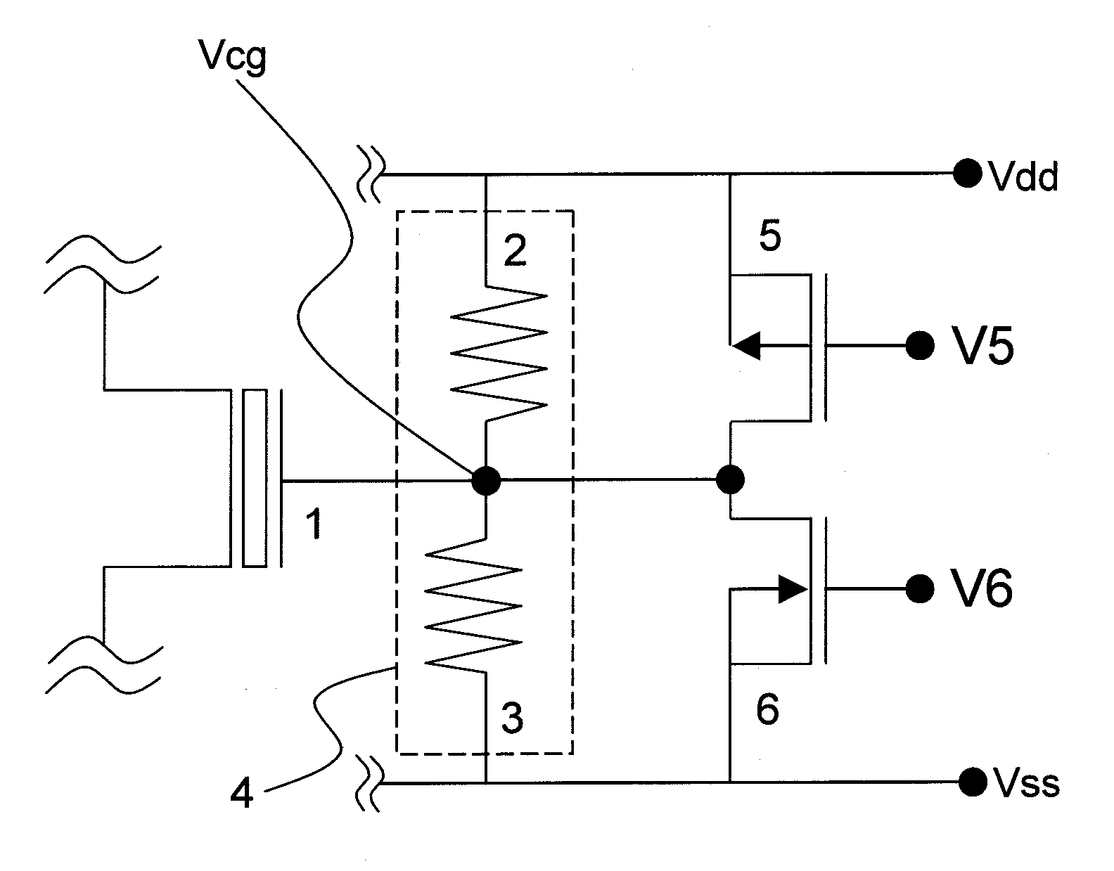
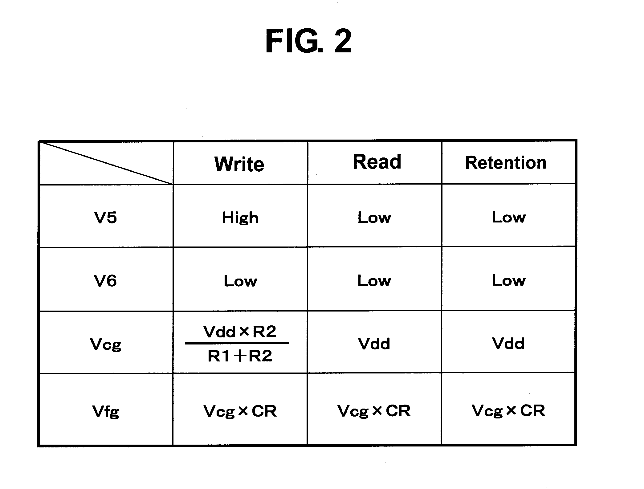
[0027]In this embodiment, as illustrated in FIG. 1, a P-channel non-volatile memory element 1 includes a floating gate and a control gate capacitively coupled to the floating gate. The control gate is connected to a divided voltage output of a resistor divider 4 including a first resistor 2 and a second resistor 3 for dividing a voltage difference between a power supply voltage and a ground voltage, and is also connected to a P-channel switch transistor 5 connected in parallel to the first resistor 2 and an N-channel switch transistor 6 connected in parallel to the second resistor 3.

[0028]Next, a description is given of the operation of the non-volatile memory circuit according to this embodiment.

[0029]The r...


PUM


Abstract

A non-volatile memory circuit is formed of a P-channel MOS transistor and includes a P-channel non-volatile memory element having a floating gate and a control gate capacitively coupled together. A resistor divider has a first resistor and a second resistor for dividing a voltage difference between a power supply voltage and a ground voltage. A divided voltage output of the resistor divider is connected to the control gate. First and second switches are connected in parallel to the respective first and second resistors. The first and second switches are controlled so that a voltage of the control gate is set to a voltage of the divided voltage output which maximizes an electric field between a pinch-off point and a drain point of the P-channel MOS transistor in a writing mode.

Description

BACKGROUND OF THE INVENTION[0001]1. Field of the Invention[0002]The present invention relates to a non-volatile memory circuit capable of electrical writing and reading.[0003]2. Description of the Related Art[0004]There is known a semiconductor integrated circuit including a bleeder resistor circuit capable of being trimmed by a memory. Hitherto, the bleeder resistance is adjusted by a method of mechanically cutting the fuse formed in parallel to the bleeder resistor with use of laser light or the like. The trimming of the bleeder resistor can accordingly be performed only before assembling a package. The use of a memory for trimming the bleeder resistor, on the other hand, enables electrical trimming even after the assembly. The following two typical benefits are obtained.[0005]1. Users' requests for quick delivery can be accommodated because the trimming is carried out for the bleeder resistor in the package before shipment.[0006]2. High precision can be achieved because the trimm...

Claims


Application Information

Patent Timeline
Patent Type & Authority Patents(United States)
IPC IPC(8): G11C11/34G11C16/12G11C16/04
CPCG11C16/12G11C16/0408G11C16/06
Inventor KAWAKAMI, AYAKOTSUMURA, KAZUHIRO
Owner ABLIC INC
Why Eureka
Try Eureka