
Hollow photovoltaic fiber

a photovoltaic fiber and hollow technology, applied in the field of hollow photovoltaic fibers, can solve the problems of reducing affecting and reducing the so as to effectively minimize or eliminate the impact of the strip contact on the energy conversion efficiency of the hollow photovoltaic fiber. , the effect of reducing the impact of the strip conta

Active Publication Date: 2015-06-09
SUNJOULE MATERIALS
View PDF7 Cites 1 Cited by
  • Summary
  • Abstract
  • Description
  • Claims
  • Application Information

AI Technical Summary

Benefits of technology

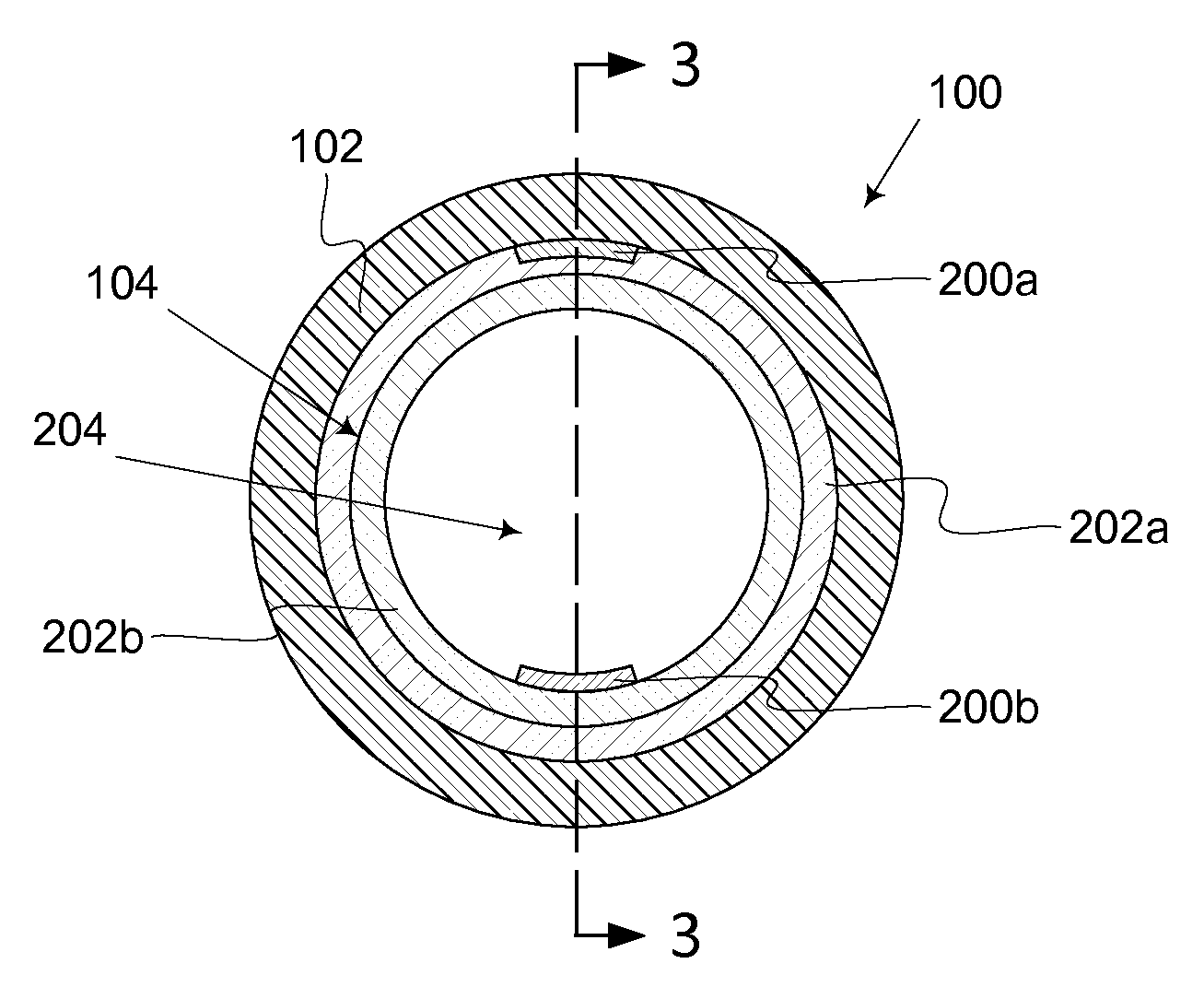
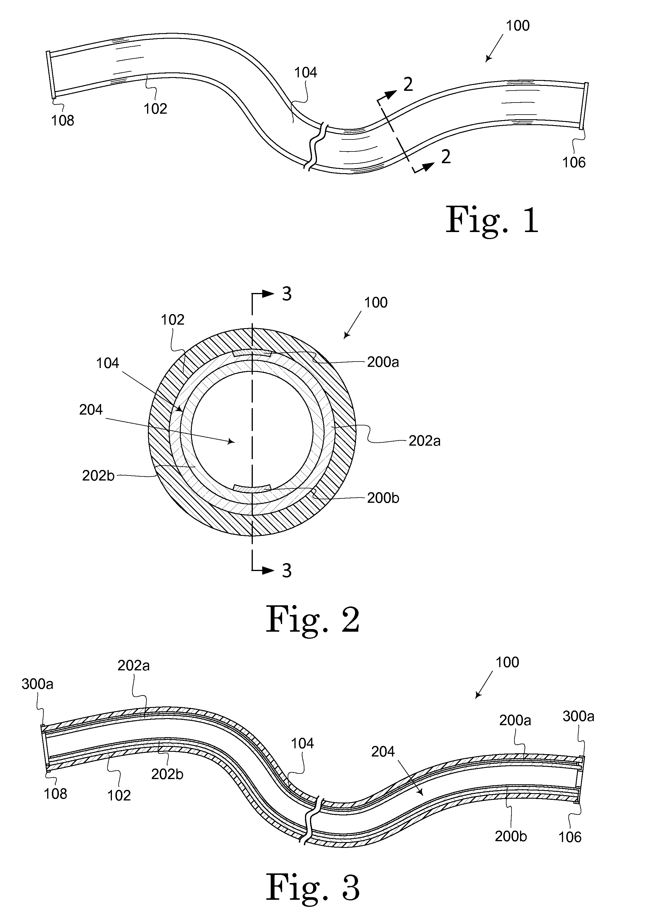
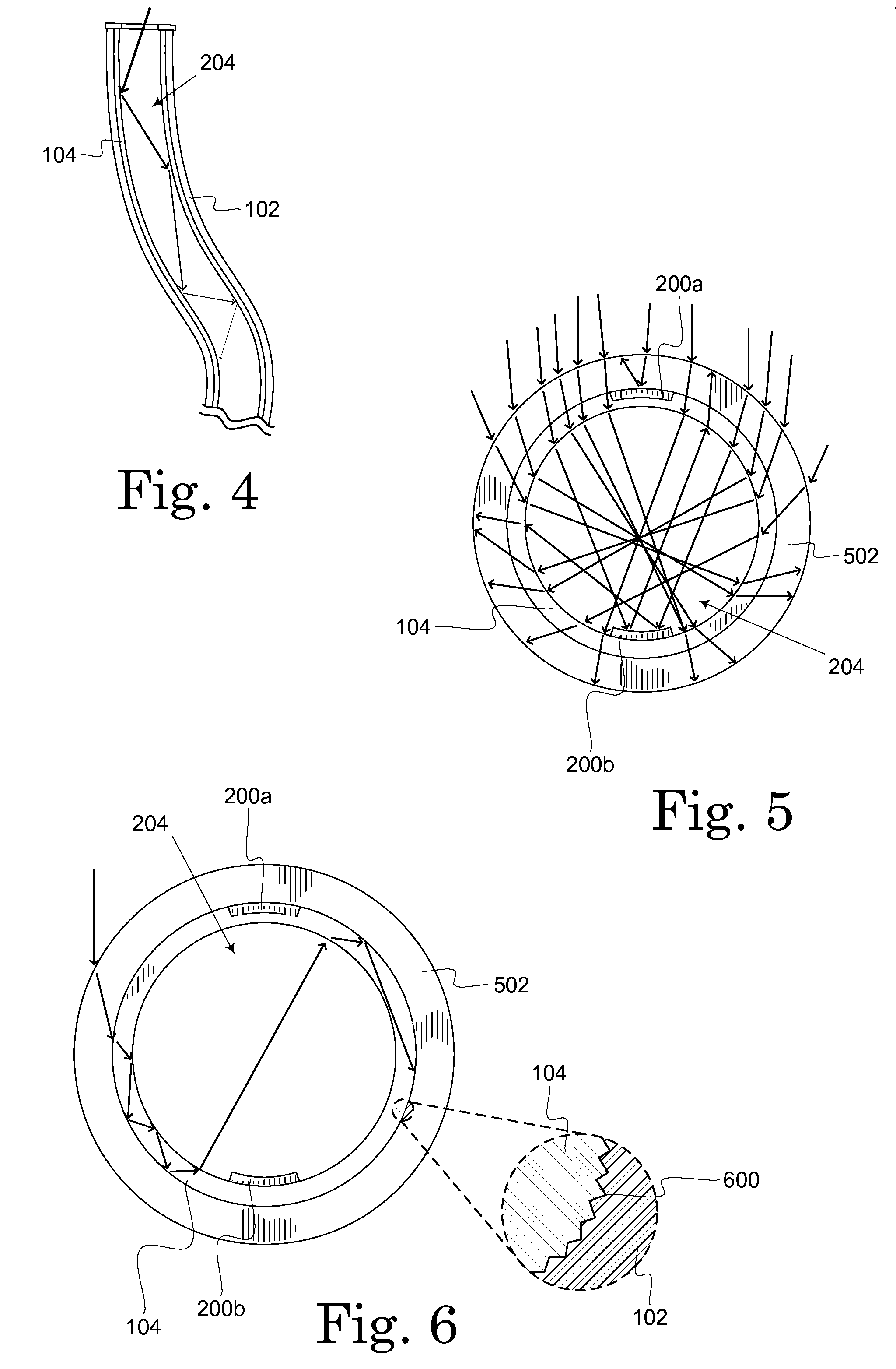
[0004]The multiple interactions between the light and the semiconductor occurring in the hollow photovoltaic fiber contribute to greater energy conversion efficiency when compared with a planar thin film solar cell. Light entering the hollow photovoltaic fiber is guided along the length of the tube and interacts with the inner surface multiple times. Each time the light interacts with the inner wall, some portion is absorbed. The remainder of the light is reflected within the tube and interacts with the inner wall at another point. Although the energy absorption during any particular interaction may be relatively small, the multiple interactions between the light and the inner wall allow the semiconductor to efficiently capture a substantial portion of the energy from the light as it travels along the tube. The multiple interactions between the light and the semiconductor effectively minimize or eliminate the impact of the strip contacts on the energy conversion efficiency of the hollow photovoltaic fiber. The multiple interactions also allow use of thinner semiconductor layers than required by planar thin film solar cells without having a significant adverse effect on the energy conversion efficiency of the hollow photovoltaic fiber.
[0005]The hollow photovoltaic fiber fabricated using a transparent substrate, absorbs light incident on the tube regardless of where the light strikes the hollow photovoltaic fiber or the angle of incidence. This allows the hollow photovoltaic fiber to operate in any orientation. With a semiconductor thickness less than or equal to 100 nm, the hollow photovoltaic fiber exhibits two-dimensional quantum mechanical effects that enhance the photovoltaic performance. The hollow photovoltaic fiber allows the production of solar cells equivalent or superior to conventional planar thin film solar cells using significantly less semiconductor and / or substrate material.

Problems solved by technology

In other words, the techniques and materials that lead to increased efficiency also lead to increased cost.
Many cost reduction techniques used with planar thin film solar cells, such as reducing the thickness of the semiconductor or eliminating materials, tend to lower efficiency, often significantly.
Conventional planar thin film solar cells commonly have complicated designs, use expensive materials, and require additional processing steps in order to approach the theoretical light trapping limit.
The complexity, specialized materials, and additional processing increase the cost of planar thin film solar cells.

Method used


Image

  • Hollow photovoltaic fiber
  • Hollow photovoltaic fiber
  • Hollow photovoltaic fiber

Examples


Embodiment Construction

[0024]A hollow photovoltaic fiber is described herein and illustrated in the accompanying figures. The hollow photovoltaic fiber includes semiconductor formed on the inner surface of a hollow tube or on a flexible substrate subsequently formed into a hollow tube. The hollow photovoltaic fiber is suitable for creating a variety of semiconductor devices, including solar cells. Light entering the hollow photovoltaic fiber deposits energy in the semiconductor as it travel through the tube. The hollow photovoltaic fiber exhibits improved energy conversion efficiency over planar thin film solar cells due to the large semiconductor surface area and longer light travel path provided by the tube. Embodiments of the hollow photovoltaic fiber are lightweight and flexible allowing the creation of non-planar solar cells and the applications for solar cells to extend into such areas as the manufacture of photovoltaic textiles or photovoltaic non-woven fabrics.

[0025]FIG. 1 illustrates one embodime...


PUM


Abstract

A hollow photovoltaic fiber. The hollow photovoltaic fiber includes semiconductor formed on the inner surface of a hollow tube or on a flexible substrate subsequently formed into a hollow tube. The hollow photovoltaic fiber is suitable a variety of semiconductor devices, including solar cells. Light entering the hollow photovoltaic fiber deposits energy in the semiconductor as it travel through the tube. The hollow photovoltaic fiber exhibits improved energy conversion efficiency over planar thin film solar cells due to the large semiconductor surface area and longer light travel path provided by the tube. Embodiments of the hollow photovoltaic fiber are lightweight and flexible allowing the creation of non-planar solar cells and the applications for solar cells to extend into such areas as the manufacture of photovoltaic textiles or photovoltaic non-woven fabrics.

Description

BACKGROUND[0001]Planar thin film solar cells (TFSC) dominate the current generation of solar cell technology. The cost and the efficiency of a planar thin film semiconductor are directly related. In other words, the techniques and materials that lead to increased efficiency also lead to increased cost. Many cost reduction techniques used with planar thin film solar cells, such as reducing the thickness of the semiconductor or eliminating materials, tend to lower efficiency, often significantly. Conventional bulk silicon (Si) solar cells have efficiencies in the range of 15% to 25%, while conventional ultrathin solar cells have efficiencies in the range of 8% to 10%. The fundamental reason for the lower efficiency of conventional ultrathin solar cells is the reduction in the amount of light trapped and absorbed resulting from the use of a thinner semiconductor.[0002]In order for the semiconductor of a planar thin film solar cell to trap light, the light must enter the semiconductor a...

Claims


Application Information

Patent Timeline
Patent Type & Authority Patents(United States)
IPC IPC(8): H01L31/0352H01L31/052H01L31/0224H01L31/0392H01L31/042
CPCH01L31/035281H01L31/022433H01L31/0392H01L31/042H01L31/0543Y02E10/52H01L31/0547H01L31/03926
Inventor KALYANARAMAN, RAMAKRISHNANKRISHNAN, VEENA GOPALGARCIA, HERNANDODUSCHER, GERDMALASI, ABHINAV
Owner SUNJOULE MATERIALS
Learn More