Non-volatile memory system with reset verification mechanism and method of operation thereof

a non-volatile memory and verification mechanism technology, applied in the field of memory systems, can solve the problems of limited life span of current flash memory devices, based on charge storage technologies, damage can be caused, block erase may have insufficient current to reset all of the individual cells in the erase block, etc., to achieve high resistance state, low resistance state, and increase read margin

Inactive Publication Date: 2015-06-30
SONY SEMICON SOLUTIONS CORP
View PDF12 Cites 38 Cited by
  • Summary
  • Abstract
  • Description
  • Claims
  • Application Information

AI Technical Summary

Benefits of technology

[0009]The present invention provides a method of operation of a non-volatile memory system including: providing a resistive storage element having a high resistance state and a low resistance state; coupling an analog multiplexer to the resistive storage element for applying a bias voltage; and switching between a verification bias and a read bias through the analog multiplexer for increasing a read margin between the high resistance state and the low resistance state.
[0010]The present invention provides a non-volatile memory system, including: a resistive storage element having a high resistance state and a low resistance state; an analog multiplexer coupled to the resistive storage element for applying a bias voltage; and a read reference generator provides a verification bias and a read bias through the analog multiplexer for increasing a read margin between the high resistance state and the low resistance state.

Problems solved by technology

The current flash memory devices, based on charge storage technologies, have limited life spans due to damage of the charge storage layers during writes.
The damage can be caused by physical weakening of the crystal structure used to store the charge.
An issue that has arisen in the new R-RAM technology is that the block erase may have insufficient current to reset all of the individual cells in the erase block.
The iterative erase cycles can consume additional power and increase background processing time.
Solutions to these problems have been long sought but prior developments have not taught or suggested any solutions and, thus, solutions to these problems have long eluded those skilled in the art.

Method used


Image

  • Non-volatile memory system with reset verification mechanism and method of operation thereof
  • Non-volatile memory system with reset verification mechanism and method of operation thereof
  • Non-volatile memory system with reset verification mechanism and method of operation thereof

Examples


Embodiment Construction

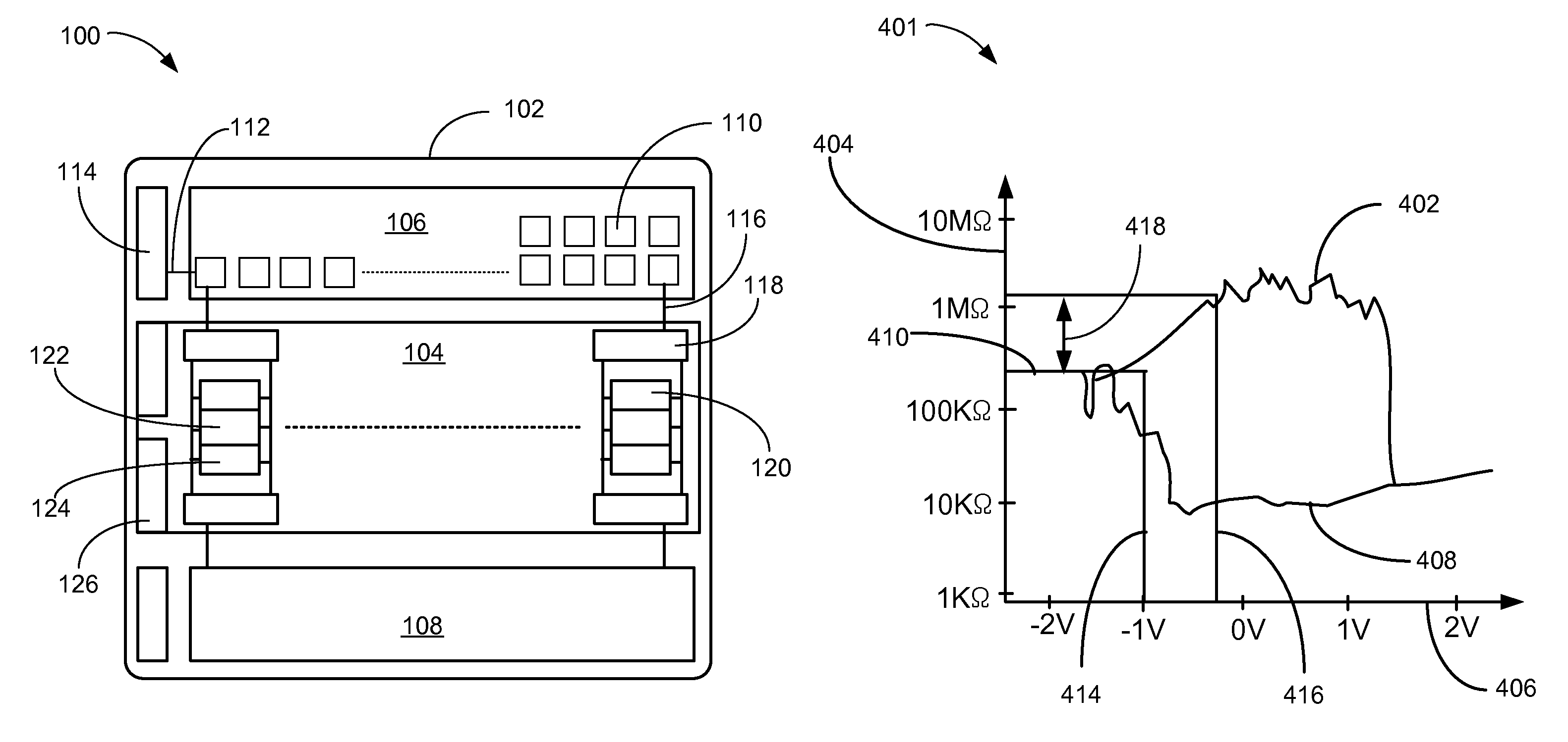
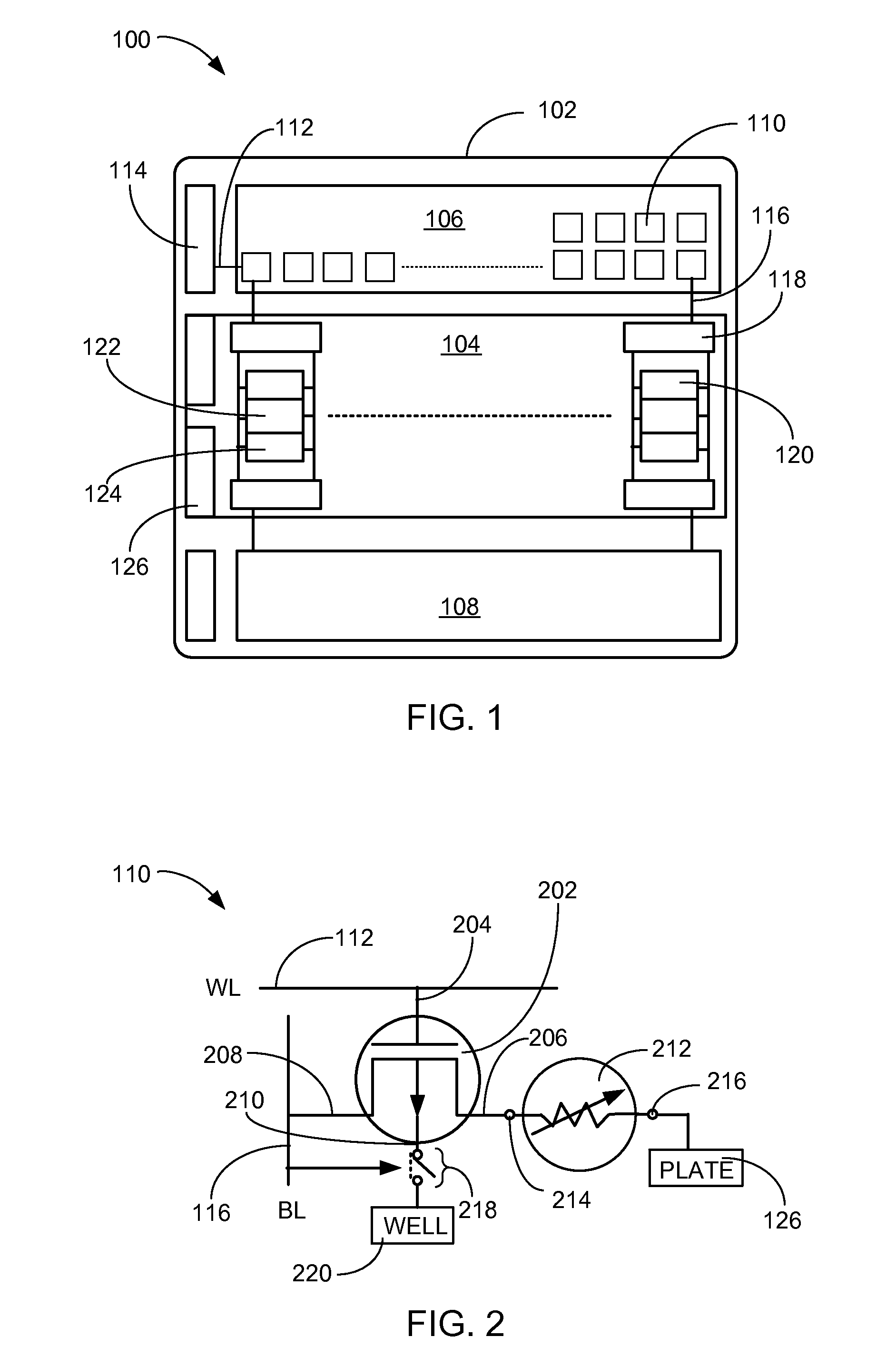
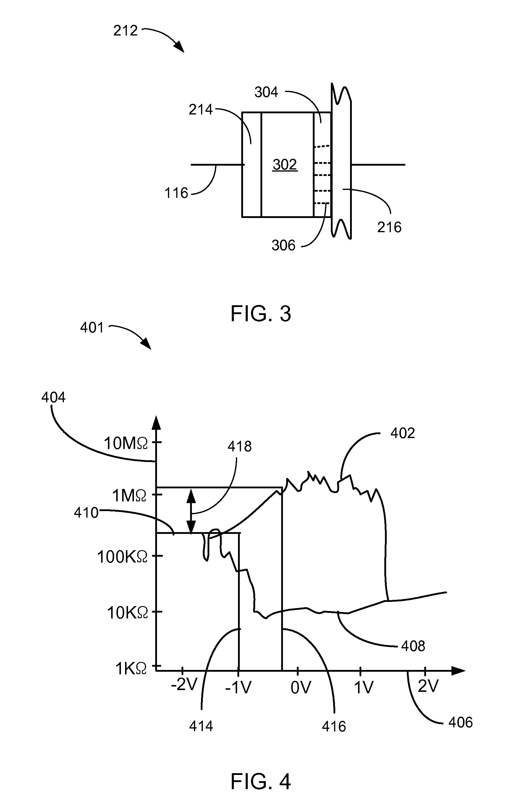
[0018]The following embodiments are described in sufficient detail to enable those skilled in the art to make and use the invention. It is to be understood that other embodiments would be evident based on the present disclosure, and that system, process, or mechanical changes may be made without departing from the scope of the present invention.

[0019]In the following description, numerous specific details are given to provide a thorough understanding of the invention. However, it will be apparent that the invention may be practiced without these specific details. In order to avoid obscuring the present invention, some well-known circuits, system configurations, and process steps are not disclosed in detail.

[0020]The drawings showing embodiments of the system are semi-diagrammatic and not to scale and, particularly, some of the dimensions are for the clarity of presentation and are shown exaggerated in the drawing FIGs. Similarly, although the views in the drawings for ease of descri...


PUM


Abstract

A method of operation of a non-volatile memory system includes: providing a resistive storage element having a high resistance state and a low resistance state; coupling an analog multiplexer to the resistive storage element for applying a bias voltage; and switching between a verification bias and a read bias through the analog multiplexer for increasing a read margin between the high resistance state and the low resistance state.

Description

TECHNICAL FIELD[0001]The present invention relates generally to a memory system, and more particularly to a system for managing group erase of individual cells in a non-volatile memory array.BACKGROUND ART[0002]The performance of non-volatile memory systems has improved over the past several years. Changes in technology management have pushed the non-volatile memory devices into cameras, computers, personal data assistants, smart phones, and proprietary business applications.[0003]The current flash memory devices, based on charge storage technologies, have limited life spans due to damage of the charge storage layers during writes. The damage can be caused by physical weakening of the crystal structure used to store the charge. This condition is countered by limiting the number of writes and reads that an individual memory cell can undergo. The limited reliability of the cells has given rise to error correction strategies and distributed write operations in order to extend the useab...

Claims


Application Information

Patent Timeline
Patent Type & Authority Patents(United States)
IPC IPC(8): G11C13/00H01L45/00
CPCG11C13/0097H01L45/146G11C13/0011G11C13/0002G11C13/003G11C13/0064G11C2213/32G11C2213/79G11C13/004H10N70/24H10N70/8416H10N70/8833G11C2013/0054
Inventor OTSUKA, WATARUSUMINO, JUNTSUSHIMA, TOMOHITOKITAGAWA, MAKOTOKUNIHIRO, TAKAFUMI
Owner SONY SEMICON SOLUTIONS CORP
Why Eureka
Try Eureka