Ferroelectric memory

Active Publication Date: 2005-05-31
OL SECURITY LIABILITY CO
View PDF2 Cites 7 Cited by
  • Summary
  • Abstract
  • Description
  • Claims
  • Application Information

AI Technical Summary

Benefits of technology

[0015]An object of the present invention is to provide a ferroelectric memory capable of suppressing false data reading or the like by increasing a read margin.

Problems solved by technology

Repetition of such polarization inversion disadvantageously results in polarization fatigue / deterioration such as reduction of remanence.
This disadvantageously results in false data reading or the like.

Method used


Image

  • Ferroelectric memory
  • Ferroelectric memory
  • Ferroelectric memory

Examples


first embodiment

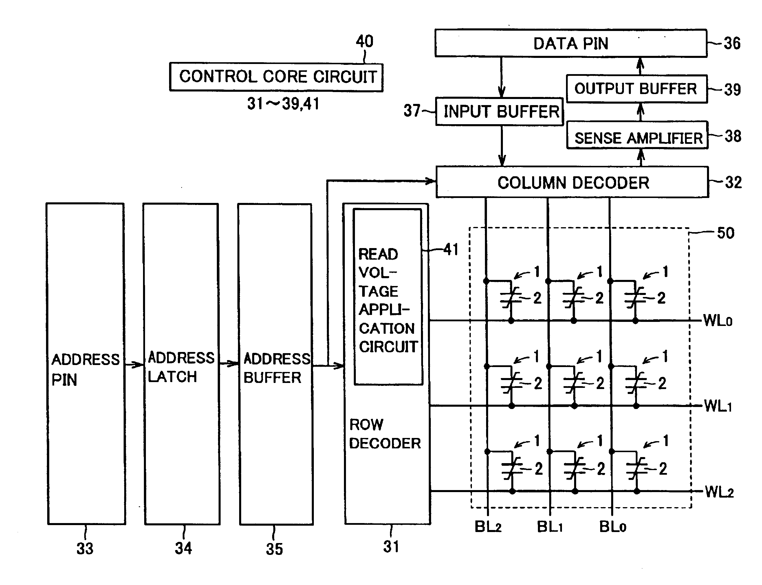
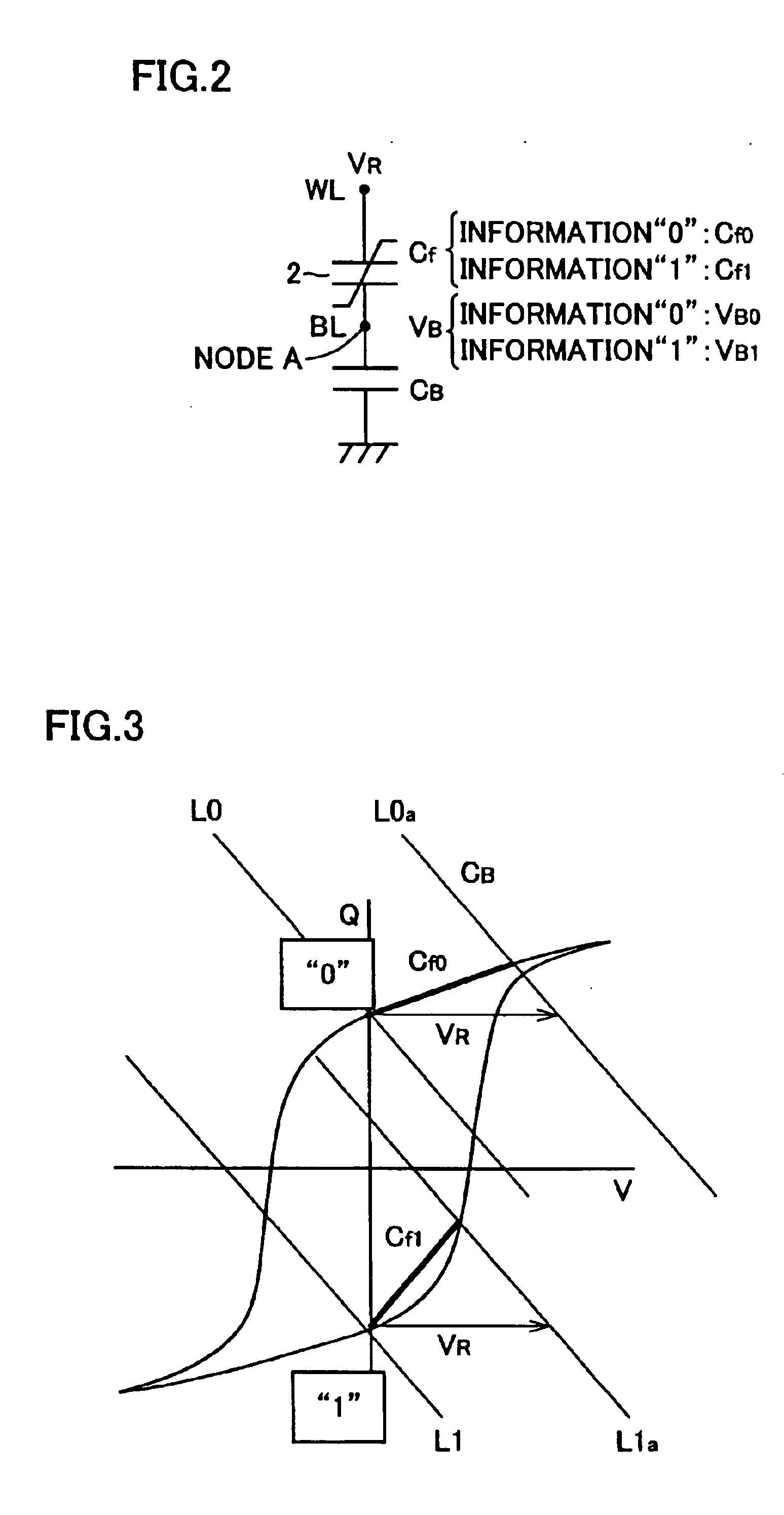
[0059]The overall structure of a simple matrix ferroelectric memory according to a first embodiment of the present invention is described with reference to FIG. 1. In the ferroelectric memory according to the first embodiment, a memory cell array 50 is constituted of a plurality of memory cells 1 arranged in the form of a matrix (for the convenience of illustration, FIG. 1 shows only nine memory cells 1). First terminals of ferroelectric capacitors 2 constituting the memory cells 1 are connected to word lines WL0 to WL2 while second terminals of the ferroelectric capacitors 2 are connected to bit lines BL0 to BL2. In other words, each memory cell 1 is constituted of only a single ferroelectric capacitor 2 in the first embodiment. Each ferroelectric capacitor 2 includes a ferroelectric film capable of taking different electric capacitances Cf0 and Cf1 in an initial state applying no voltage.

[0060]The word lines WL0 to WL2 are connected to a row decoder 31. The bit lines BL0 to BL2 ar...

second embodiment

[0089]Referring to FIGS. 7 and 8, a second embodiment of the present invention is applied to a 1T1C ferroelectric memory.

[0090]According to the second embodiment, a memory cell array 60 is constituted of a plurality of memory cells 11 arranged in the form of a matrix, as shown in FIG. 7 (for the convenience of illustration, FIG. 7 shows only nine memory cells 11). Each memory cell 11 is constituted of a single ferroelectric capacitor 12 and a single switching transistor 13. A first electrode of the ferroelectric capacitor 12 is connected to any of plate lines PL0 to PL2 while a second electrode thereof is connected to either one of source / drain regions of the switching transistor 13. The other source / drain region of the switching transistor 13 is connected to any of bit lines BL0 to BL2. The gate electrode of the switching transistor 13 is connected to any of word lines WL0 to WL2. A row decoder 31 stores a read voltage application circuit 41a for applying a read voltage VR to the p...

third embodiment

[0093]Referring to FIGS. 9 and 10, a third embodiment of the present invention is applied to an FET ferroelectric memory.

[0094]In the FET ferroelectric memory according to the third embodiment, a memory cell array 70 is constituted of a plurality of memory cells 21 arranged in the form of a matrix (for the convenience of illustration, FIG. 9 shows only nine memory cells 21). Each memory cell 21 is constituted of a single transistor (FET) 23 and a ferroelectric capacitor 22 formed on the gate portion of the transistor 23. A first electrode of the ferroelectric capacitor 22 is connected to any of word lines WL0to WL2 while a second electrode thereof is connected to the gate electrode of the transistor 23. One of source / drain regions of the transistor 23 is connected to any of bit lines BL0 to BL2, and the other source / drain region is connected to any of plate lines PL0 to PL2. A channel region (well region) of the transistor 23 is connected to any of source lines SL0 to SL2.

[0095]Acco...


PUM


Abstract

A ferroelectric memory capable of suppressing false data reading or the like by increasing a read margin is obtained. This ferroelectric memory comprises a circuit applying a read voltage VR to a first electrode and a detector capable of detecting the difference between electric capacitances Cf0 and Cf1 of a ferroelectric film when the potential difference of a second electrode corresponding to the difference between the electric capacitances Cf0 and Cf1 of the ferroelectric film is in excess of a detection limit voltage VS. The electric capacitance C2 of the second electrode is set to satisfy the following expression:Cf0<C2≦½×{(Cf1−Cf0)VR / VS−(Cf1+Cf0)}.

Description

BACKGROUND OF THE INVENTION[0001]1. Field of the Invention[0002]The present invention relates to a ferroelectric memory, and more particularly, it relates to a ferroelectric memory having a ferroelectric capacitor.[0003]2. Description of the Background Art[0004]A ferroelectric memory has recently been watched with interest as a high-speed nonvolatile memory requiring low power consumption. Therefore, the ferroelectric memory is subjected to active research and development.[0005]FIG. 11 is a representative circuit diagram of a most generally employed conventional 1T1C ferroelectric memory, and FIG. 12 is a sectional view corresponding to FIG. 11. Referring to FIGS. 11 and 12, element isolation regions 102 are formed on prescribed regions of the surface of a semiconductor substrate 101 in the structure of this conventional 1T1C ferroelectric memory. Source regions 103 and a drain region 104 are formed at prescribed intervals on an element forming region enclosed with the element isola...

Claims


Application Information

Patent Timeline
IPC IPC(8): G11C11/22H01L21/70H01L29/66H01L21/8247H01L29/788H01L27/105H01L29/792G11C8/08H01L21/8246
CPCG11C11/22G11C8/08E01D21/00E01H1/103
Inventor MATSUSHITA, SHIGEHARU
Owner OL SECURITY LIABILITY CO
Why Eureka
Try Eureka