Semiconductor memory device

a memory device and semiconductor technology, applied in the field of semiconductor memory devices, can solve the problems of inability to stably keep data of ‘1’, difficulty in keeping data for a long period of time, etc., and achieve the effect of improving the reliability of the device operation, increasing the read margin, and increasing the exactness of the read operation

Inactive Publication Date: 2005-06-09
SK HYNIX INC
View PDF7 Cites 4 Cited by
  • Summary
  • Abstract
  • Description
  • Claims
  • Application Information

AI Technical Summary

Benefits of technology

[0013] An object of the present invention is to provide semiconductor memory device capable of increasing the exactness of the read operation and improving reliability of the device operation by increasing a read margin, in such a manner that a word line selected in the process in which the memory cell reads stored data and a word line neighboring it are simultaneously selected, or two bit lines (or inverted bit lines) are simultaneously connected to the input terminal of the sense amplifier to increase the difference in the voltage between both input terminals of the sense amplifier.
[0027] The semiconductor memory device of the present invention constructed above simultaneously selects two bit lines or two word line neighboring each other to simultaneously connected them to the input terminal of the sense amplifier, and then increases the difference in voltage between the both input terminals of the sense amplifier, in a normal operation or a refresh operation. Therefore, a read margin could be increased, the exactness of a read operation could be increased and reliability of the device operation could be improved.

Problems solved by technology

At the same time, there occur several problems for the memory cell to store data.
For this reason, there is a difficulty in keeping data for a long period of time.
However, in case where data of ‘1’ is stored since the charge is charged into the capacitor of the memory cell, data of ‘1’ could not be stably kept since the charged charge is discharged as time goes.
If the difference in the voltage (a) is not high, read error may occur.
Due to this, there is a problem that current consumption and the defective rate are increased.

Method used


Image

  • Semiconductor memory device
  • Semiconductor memory device
  • Semiconductor memory device

Examples


first embodiment

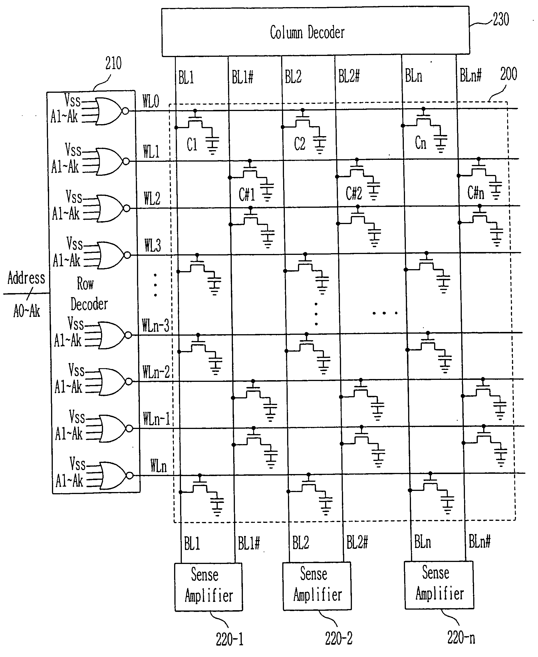
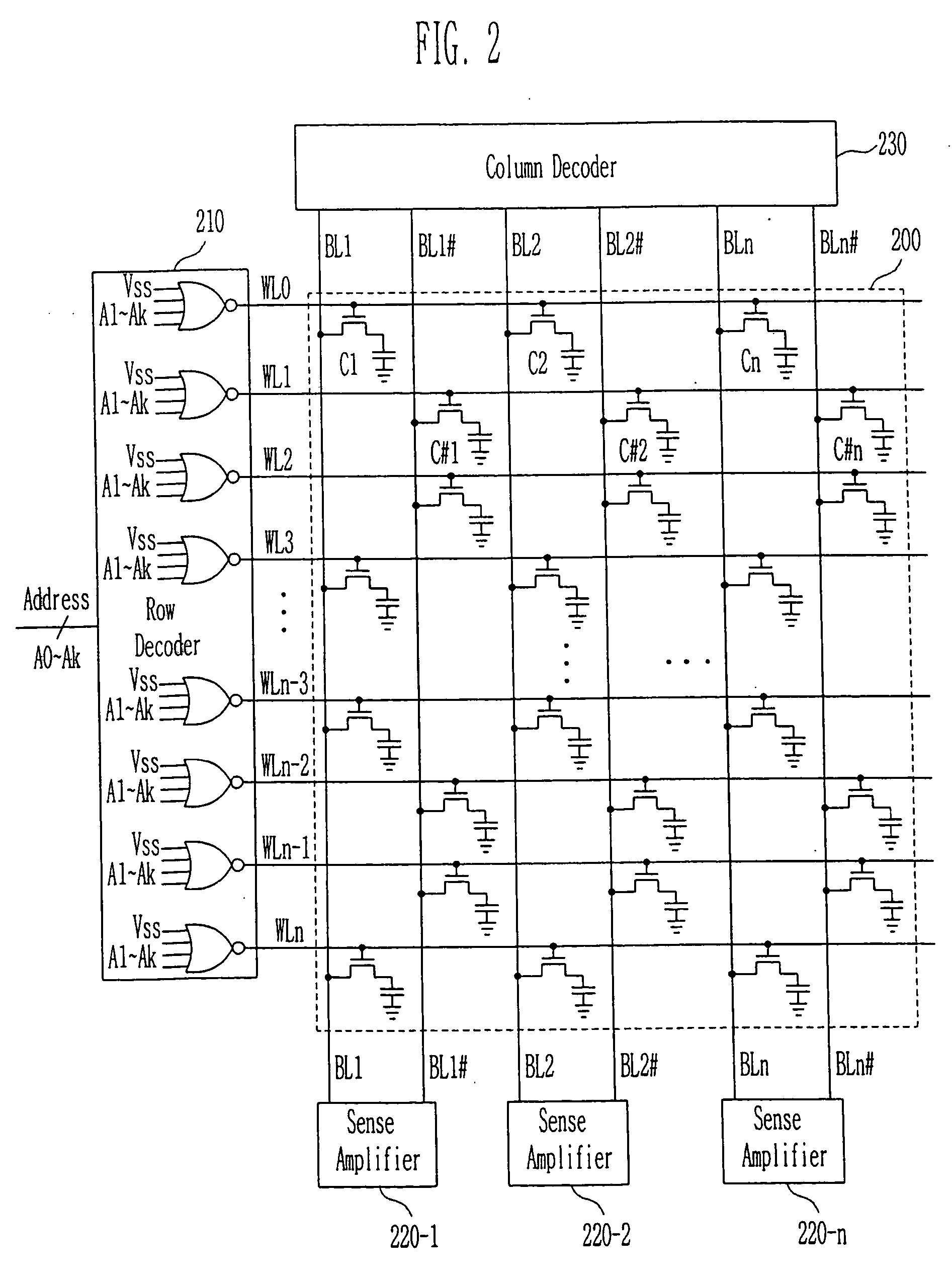
[0038]FIG. 2 is a circuit diagram for explaining connection relationship and operation of a semiconductor memory device according to the present invention.

[0039] Referring to FIG. 2, in the semiconductor memory device according to the first embodiment of the present invention, a memory cell array 200, sense amplifiers 220-1˜220 -n, a column decoder 230 and peripheral circuits (not shown) are same to the conventional ones. For simplicity, explanation on them will be omitted.

[0040] Meanwhile, in the normal operation or refresh operation, as one of methods for simultaneously selecting two neighboring word lines, the two neighboring word lines may be simultaneously selected by changing an internal circuit of the row decoder 210. An operation of simultaneously selecting the internal circuit of the row decoder 210 and two neighboring word lines will be described by reference to the drawings.

[0041]FIG. 3 illustrates the internal circuit of the row decoder shown in FIG. 2.

[0042] By refer...

second embodiment

[0049]FIG. 4 is a circuit diagram for explaining connection relationship and operation of the semiconductor memory device according to the present invention.

[0050] Referring to FIG. 4, all connection relationship are same to those in the semiconductor memory device described by reference to FIG. 2 but arrangement of the true cells C1˜Cn and C′1˜C′n and the complement cells C#1˜C#n are quite different. In the concrete, in FIG. 2, if two word lines neighboring each other are selected, the memory cell is arranged in one word line such that the word line to which the true cell is connected and the word line to which the complement cell is connected are selected at the same time. As in FIG. 4, however, the memory cell may be arranged such that the two neighboring word lines to which only the true cell or the complement cell is connected may be selected at the same time.

[0051] If the two word lines adjacent to the address signals A0˜Ak are simultaneously enabled by the row decoder 210, t...

third embodiment

[0054]FIG. 5 is a circuit diagram for explaining connection relationship and operation of the semiconductor memory device according to the present invention. FIG. 6 illustrates an internal circuit of the row decoder shown in FIG. 5.

[0055] The third embodiment of FIG. 5 is same to the second embodiment of FIG. 2 except that only the remaining addresses A1˜Ak of the addresses A0˜Ak except for the lowest address A0 are decoded to generate the word line select signal and that the word line select signal generated in the row decoder 210 selects the two word lines at the same time. This will be explained in detail below.

[0056] In the third embodiment, only the addresses A1˜Ak except for the lowest address A0 are decoded to generate a signal for selecting the word line. At this time, if only the remaining addresses A1˜Ak except for the lowest address A0 are decoded, the number of the NOR gate is reduced by half and the size of the row decoder 210 is thus reduced. However, the number of th...


PUM


Abstract

Disclosed is a semiconductor memory device. In the process for the memory cell to reading stored data by selecting specific word lines, word lines neighboring the selected word line are selected at the same time, or the two bit lines are connected at the same time to the input terminals of the sense amplifiers, thus increasing the difference in voltage between both the input terminals of the sense amplifiers. Therefore, the read margin is increased, the exactness of the read operation is increased, and reliability of the device is improved.

Description

BACKGROUND OF THE INVENTION [0001] 1. Field of the Invention [0002] The present invention relates to a semiconductor memory device, and more particularly, to a semiconductor memory device capable of improving reliability of the device by increasing a margin of the read operation for reading data stored at the memory cell. [0003] 2. Background of the Related Art [0004] As the degree of integration in the device is increased, the area of the memory cell is reduced. At the same time, there occur several problems for the memory cell to store data. [0005] For example, in case of a DRAM, the memory cell consists of one transistor and one capacitor. Data is stored at the memory cell by a method of charging or discharging the charge into or from the capacitor. In this case, as the size of the capacitor is reduced in order to increase the degree of integration in the degree, time when the charge stored at the capacitor is discharged is shortened. For this reason, there is a difficulty in kee...

Claims


Application Information

Patent Timeline
Patent Type & Authority Applications(United States)
IPC IPC(8): G11C11/409G11C7/06G11C7/10G11C7/18G11C8/10G11C11/408G11C11/4091G11C11/4097
CPCG11C7/062G11C7/1051G11C7/18G11C11/4097G11C11/4087G11C11/4091G11C8/10G11C11/409
Inventor CHOI, GUG SEON
Owner SK HYNIX INC
Why Eureka
Try Eureka