Image sensor and fabricating method of image sensor

a technology of image sensor and fabricating method, which is applied in the direction of electrical equipment, semiconductor devices, radio frequency control devices, etc., can solve the problems of high requirements for automobile image sensor, many details must be buried, and high undesirable blooming, so as to reduce the effect of blooming

Active Publication Date: 2015-06-30
HIMAX IMAGING LIMITED
View PDF7 Cites 4 Cited by
  • Summary
  • Abstract
  • Description
  • Claims
  • Application Information

AI Technical Summary

Benefits of technology

[0013]It is therefore one of the objectives of the present invention to provide an image sensor and a fabricating method of the image sensor capable of reducing blooming by forming an anti-blooming path between the source follower transistor channel and the photodiode region, so as to solve the above problem because normally the SF drain is connected to the most positive power supply available on chip, so it acts as a very effective drain of blooming current injected into SF channel.
[0016]Briefly summarized, the image sensor and the fabricating method of the image sensor of the present invention are capable of reducing blooming by forming an anti-blooming path between the source follower transistor channel and the photodiode region and with no STI between the source follower transistor channel and the photodiode region. By proper tuning of anti-blooming path potential barrier, almost all the electron leakage current generated from SF channel depletion region will be absorbed by SF drain terminal. Thus, the present invention can solve the above problem of using the Tx gate as the anti-blooming drain.

Problems solved by technology

However, the requirements to an automobile image sensor are very demanding.
Blooming is highly undesirable in CIS applications, especially automotive and surveillance ones.
Otherwise, many details must be buried and it is hard for the car control system or the driver to extract the information from the scene.
The blooming of a longer integration PD could destroy the information in the shorter integration one.
1, January 1984), the CCD solution can provide high voltage for solid control of veridical drain “on” an “off” but such a large range of voltage is not available for the CIS.
However, this solution has disadvantages of high leakage current from the Tx channel to the PD region, and increasing dark current and white pixels dramatically, and FWC is also a trade-off in this scheme.

Method used


Image

  • Image sensor and fabricating method of image sensor
  • Image sensor and fabricating method of image sensor
  • Image sensor and fabricating method of image sensor

Examples


Embodiment Construction

[0026]Certain terms are used throughout the following description and claims to refer to particular components. As one skilled in the art will appreciate, hardware manufacturers may refer to a component by different names. This document does not intend to distinguish between components that differ in name but in function. In the following discussion and in the claims, the terms “include”, “including”, “comprise”, and “comprising” are used in an open-ended fashion, and thus should be interpreted to mean “including, but not limited to . . . ”.

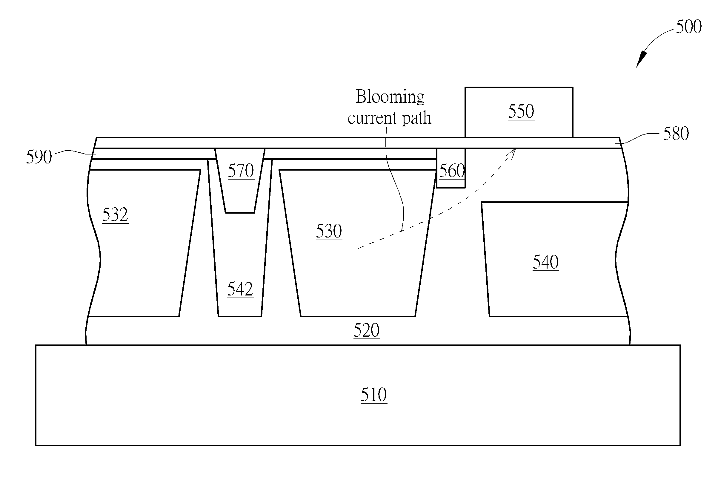
[0027]Please refer to FIG. 6. FIG. 6 shows a simplified cross-sectional view diagram of an image sensor 500 according to an embodiment of the present invention. As shown in FIG. 6, the image sensor 500 comprises: a P type substrate 510, a P type epitaxial layer 520, two photodiode regions 530, 532, two P type well regions 540, 542, agate region 550 of a source follower transistor, a P type implant isolation region 560, a STI 570 region, a MOS gat...


PUM


Abstract

The present invention provides an image sensor and a fabricating method of the image sensor. The image sensor comprises: a first type epitaxial layer, a photodiode region, a first type well region, a gate region of a source follower transistor, and a first type implant isolation region. The first type well region is formed within the first type epitaxial layer with a first horizontal distance to the photodiode region and a vertical distance to a surface of the first type epitaxial layer. The gate region of a source follower transistor is formed on the surface of the first type epitaxial layer and above the first type well region, and has a second horizontal distance to the photodiode region. There is a distance between the first type implant isolation region and the first type well region as an anti-blooming path.

Description

CROSS REFERENCE TO RELATED APPLICATIONS[0001]This application claims the benefit of U.S. Provisional Application No. 61 / 866,550, filed on Aug. 16, 2013 and included herein by reference.BACKGROUND OF THE INVENTION[0002]1. Field of the Invention[0003]The present invention relates to an image sensor and a fabricating method of the image sensor, and more particularly, to an image sensor and a fabricating method of the image sensor capable of reducing blooming by forming an anti-blooming path between the source follower transistor channel and the photodiode region.[0004]2. Description of the Prior Art[0005]CMOS image sensor (CIS) has been widely adopted in many applications, such as cell phone, webcam, security, toy, medical device, etc. The next big wave of CIS is on the automotive application. It can be used as driver's visual and action assistants for a safe and less stressful driving experience.[0006]However, the requirements to an automobile image sensor are very demanding. They are...

Claims


Application Information

Patent Timeline
Patent Type & Authority Patents(United States)
IPC IPC(8): H01L27/146H01L31/113H01L31/0352H01L31/18
CPCH01L31/0352H01L31/18H01L27/14654H01L27/14689H01L31/1136H01L27/14616H01L27/1463
Inventor WU, YANGYU, FEIXIAPATRICK, INNACHEUNG, YU HIN DESMOND
Owner HIMAX IMAGING LIMITED
Why Eureka
Try Eureka