Method and apparatus for optically measuring by interferometry the thickness of an object

an optical measurement and interferometer technology, applied in the direction of semiconductor/solid-state device testing/measurement, lapping machines, instruments, etc., can solve the problems of damage to the slice of semiconductor material, inability to measure very thin thicknesses, and limited technology in the dimensions they can measure. , to achieve the effect of convenient and cheap implementation

Active Publication Date: 2015-07-14
MARPOSS SPA
View PDF14 Cites 0 Cited by
  • Summary
  • Abstract
  • Description
  • Claims
  • Application Information

AI Technical Summary

Benefits of technology

[0017]Object of the present invention is to provide a method and an apparatus for optically measuring by interferometry the thickness of an object that overcome the above described inconveniences and can be easily and cheaply implemented at the same time.

Problems solved by technology

This measuring technology can cause damage to the slice of semiconductor material during the measurement owing to the mechanical contact with the mechanical feelers, and does not enable to measure very thin thicknesses (typically lower than 100 micron).
However, these technologies are limited both in the dimensions they can measure and in the highest resolution they can achieve.
But the above-mentioned analysis does not enable to determine the path followed by the reflected radiations that are combined.
But in the known apparatuses it is not possible to use information that could be present in the combinations of reflected radiations to directly or indirectly measure the distance between the optical probe and each of the discontinuity surfaces causing the reflections.
As a consequence, the analysis of the combinations of radiations reflected by the slice of semiconductor material enables to determine the measure of the thickness of the layers placed between couples of optical discontinuity surfaces, but it is not possible to determine the part of the slice of semiconductor material to which the measure of the thickness has to be assigned (that is to determine whether the measure of the thickness has to be assigned to a first layer that has been crossed twice, to the first layer that has been crossed n times, to a second or third layer, or to the first layer added to the second layer, etc.).
Therefore, the measures of a plurality of different thicknesses are determined, but it is not possible to assign each measure of thickness to a specific part or layer of the slice of semiconductor material.
However, some known recognition algorithms, as the one described above, have several inconveniences.
First of all, the accuracy of the known recognition algorithm described above is not optimal and extremely variable over time: the recognition algorithm is accurate when there are no foreign thickness values that are similar to the wanted thickness value, but it is much less accurate when there are foreign thickness values that are similar to the wanted thickness value.
The intervention of an experienced operator is normal and thus acceptable in laboratory measurements but is not possible in measurements carried out in a production line during the serial production.

Method used


Image

  • Method and apparatus for optically measuring by interferometry the thickness of an object
  • Method and apparatus for optically measuring by interferometry the thickness of an object
  • Method and apparatus for optically measuring by interferometry the thickness of an object

Examples


first embodiment

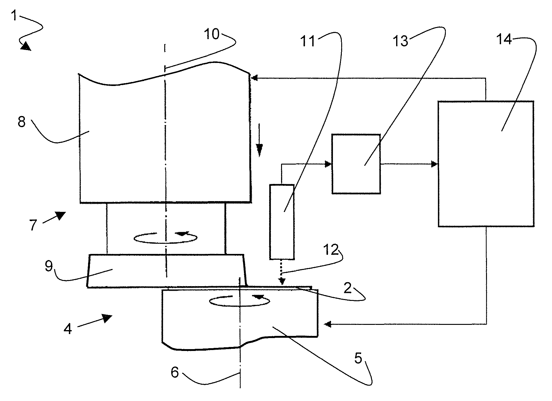
[0055] the processing unit 13 determines the minimum Tmin and the maximum Tmax of the actual value of the thickness T of the slice 2 of semiconductor material, i.e. it determines the amplitude ΔT of the variation range of the actual value of the thickness T of the slice 2 of semiconductor material as a function of a minimum and a maximum of the rough thickness values RTW belonging to the preponderant group GMAX of thickness classes C. Said minimum and maximum can be estimated, for example, on the basis of processing on the standard deviation in the distribution of such rough thickness values RTW. In other words, the rough thickness value that is estimated to be the lowest among the rough thickness values RTW belonging to the preponderant group GMAX of thickness classes C represents the minimum Tmin of the actual value of the thickness T of the slice 2 of semiconductor material, whereas the rough thickness value that is estimated to be the highest among the rough thickness values RTW...

second embodiment

[0067] measurements of the thickness T of the slice 2 of semiconductor material are carried out in a sequence, and the processing unit 13 updates the lower reject threshold Rmin and the higher reject threshold Rmax used for the current measurement of the thickness T as a function of the actual value of the thickness T determined at the end of the preceding measurement of the thickness T. Preferably, the processing unit 13 determines, according to the above described method, at each measurement of the thickness T of the slice 2 of semiconductor material the amplitude ΔT of the variation range of the actual value of the thickness T of the slice 2 of semiconductor material, too, and sets the lower reject threshold Rmin and the higher reject threshold Rmax, used for the current measurement of the thickness T of the slice 2 of semiconductor material, by subtracting from and adding to, respectively, the actual value of the thickness T determined at the end of the preceding measurement hal...


PUM

PropertyMeasurementUnit
thicknessesaaaaaaaaaa
thicknessaaaaaaaaaa
thicknessaaaaaaaaaa

Abstract

Methods and apparatuses are used for optically measuring by interferometry the thickness (T) of an object (2) such as a slice of semiconductor material. Readings of the object thickness by optical interferometry are carried out, rough thickness values (RTW) are obtained and frequencies, indicating how often the rough thickness values occur, are evaluated. A limited set of adjacent rough thickness values whose frequency integration or summation represents an absolute maximum is identified, and the actual value of the thickness of the object is determined as a function of the rough thickness values belonging to said limited set of values. The rough thickness values can be divided up into classes (C) with corresponding frequencies (F), and in this case, a preponderant group (Gmax) of thickness classes is identified as the above-mentioned limited set of adjacent rough thickness. A lower reject threshold (Rmin) and a higher reject threshold (Rmax) that define a searching interval including the actual value of the object thickness are also determined, and all the rough thickness values that are outside the searching interval are eliminated from further processing. When measuring the object during a surface machining, the reject thresholds are progressively and automatically updated as a function of a gradual thickness reduction that the object undergoes.

Description

TECHNICAL FIELD[0001]The present invention relates to a method and an apparatus for optically measuring by interferometry the thickness of an object.[0002]The present invention can be advantageously applied for optically measuring by interferometry the thickness of slices, or wafers, made of semiconductor material (typically silicon), to which reference will be explicitly made in the specification without loss of generality.BACKGROUND ART[0003]A slice of semiconductor material is machined, for example, to obtain integrated circuits or other electric components in the semiconductor material. In particular, when the slice of semiconductor material is very thin, the slice of semiconductor material is placed on a support layer (typically made of plastic material or glass) that serves to provide a higher mechanical sturdiness and thus an ease in handling.[0004]In general it is necessary to mechanically machine the slice of semiconductor material by grinding and polishing to obtain a thic...

Claims


Application Information

Patent Timeline
Patent Type & Authority Patents(United States)
IPC IPC(8): B24B1/00G01B11/06B24B7/22B24B37/013B24B49/12
CPCB24B7/228B24B37/013B24B49/12G01B11/0675G01B11/0683G01B11/0625B24B37/04H01L22/00
Inventor GALLETTI, DINOMALPEZZI, DOMENICO
Owner MARPOSS SPA
Why Eureka
Try Eureka