Shielding 2-cycle half-page read and program schemes for advanced NAND flash design

Inactive Publication Date: 2015-07-21
APLUS FLASH TECH
View PDF40 Cites 2 Cited by
  • Summary
  • Abstract
  • Description
  • Claims
  • Application Information

AI Technical Summary

Benefits of technology

[0013]An object of this invention is to provide a circuit of NAND cell string within the NAND block of NAND array to allow the highly effective BL shielding 2-cycle half-page read operation to eliminate the noise coupling between any adjacent BLs with very tight layout spacing and without any process change.
[0027]More specifically, an embodiment of this invention provides the novel BL shielding effect between any adjacent odd and even BL pairs in the selected page during NAND page read operation. As a result, any adjacent BL noise-coupling's induced errors can be prevented when NAND page reading is performed in units of half-page with two read cycles, rather than in unites of a whole page. In addition, the WL-induced threshold voltage level Vt disturbance in the selected page is also reduced during NAND's page read operation. Although there is a drawback of two cycles of half-page read to replace 1-cycle of full-page read such that the read speed is halved, but the advantage of half-page shielding read is justified due to the read data guaranteed to be immunized from the coupling-error when NAND technology migrates towards 1×nm, which has a severe read coupling effect between two very tight BL-spacing.

Problems solved by technology

Secondly, NAND Flash memory cell design uses a low-current Fowler-Nordheim (FN) tunneling phenomena for both program and erase operations.

Method used


Image

  • Shielding 2-cycle half-page read and program schemes for advanced NAND flash design
  • Shielding 2-cycle half-page read and program schemes for advanced NAND flash design
  • Shielding 2-cycle half-page read and program schemes for advanced NAND flash design

Examples


Embodiment Construction

[0043]The present invention relates generally to nonvolatile memory technology. More particularly, the present invention relates to a new 2-cycle page-read operation for NAND flash memory by providing a BL shielding effect between odd and even BLs. Applications of the present invention can be expanded to existing NAND design and further to an improved HiNAND string and array by dividing traditional 1-cycle one-page read operation into 2-cycle half-page read operation, though more applications may be recognized on all Nonvolatile memory (NVM) cells that are using the traditional on-chip compact LV page buffer, SA design, and HV charge-pump circuits.

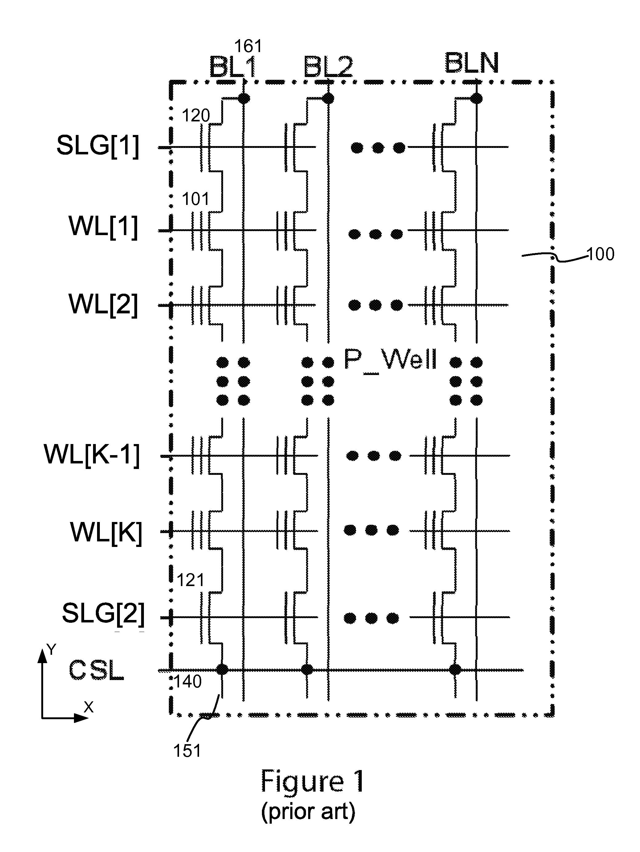
[0044]FIG. 1 is a schematic diagram of prior art of a block of the conventional NAND memory array that comprises N vertical NAND strings. Presenting this conventional NAND memory block diagram is merely used as part of an inventive process as described below. As seen, each NAND string 151 comprises K flash cells made of 2-poly floating-gat...


PUM


Abstract

The present invention provides a two-cycle half-page read scheme by dividing whole NAND array bit lines (BLs) into an odd-BL group and an even-BL group. During the half-plane reading of NAND cells in the odd(even)-BL group, the half-plane even(odd)-BL group acts as the shielding BLs to protect over the odd(even)-BL string reading so that each half-page read operation is substantially reliable and free from BL coupling noise effect. Additionally, each half-page read operation is preferably divided into 3 periods: the first being a bias-condition setup period of the selected WL and remaining control signals; the second being a pre-charge period for all BLs; and the third being a half-page flash data sensing period.

Description

CROSS-REFERENCES TO RELATED APPLICATIONS[0001]This application claims priority to U.S. Provisional Patent Application No. 61 / 687,227, filed on Apr. 20, 2012, commonly assigned, and hereby incorporated by reference in its entirety herein for all purposes.[0002]This application is related to U.S. patent application Ser. No. 13 / 843,642, filed on Mar. 15, 2013, U.S. patent application Ser. No. 13 / 680,286, filed on Nov. 19, 2012, and PCT Application No. PCT / US2012 / 065734, filed on Nov. 18, 2012, commonly assigned, and hereby incorporated by reference in its entirety herein for all purposes.BACKGROUND OF THE INVENTION[0003]The present invention relates generally to nonvolatile memory technology. More particularly, the present invention relates to a new 2-cycle page-read operation for NAND flash memory by providing a BL shielding effect between odd and even BLs. Applications of the present invention can be expanded to existing NAND design and further to an improved HiNAND string and array ...

Claims


Application Information

Patent Timeline
Patent Type & Authority Patents(United States)
IPC IPC(8): G11C16/26G11C16/04G11C16/34G11C16/24G11C11/56
CPCG11C16/26G11C16/0408G11C16/0483G11C11/5642G11C16/24G11C16/3427
Inventor LEE, PETER WUNG
Owner APLUS FLASH TECH
Why Eureka
Try Eureka