Organic light-emitting display apparatus and manufacturing method thereof

a technology of light-emitting display and organic light-emitting technology, which is applied in the direction of transistors, electroluminescent light sources, electric lighting sources, etc., can solve the problems of ineffective use, fine metal masks, and inefficient manufacturing of large-sized panels, and achieve the effect of reducing resistan

Active Publication Date: 2015-07-21
SAMSUNG DISPLAY CO LTD
View PDF7 Cites 26 Cited by
  • Summary
  • Abstract
  • Description
  • Claims
  • Application Information

AI Technical Summary

Benefits of technology

[0008]One or more exemplary embodiments of the invention include an organic light-emitting display apparatus that may easily form a pattern of a cathode as an upper electrode and may reduce resistance, and a manufacturing method of the organic light-emitting display apparatus.
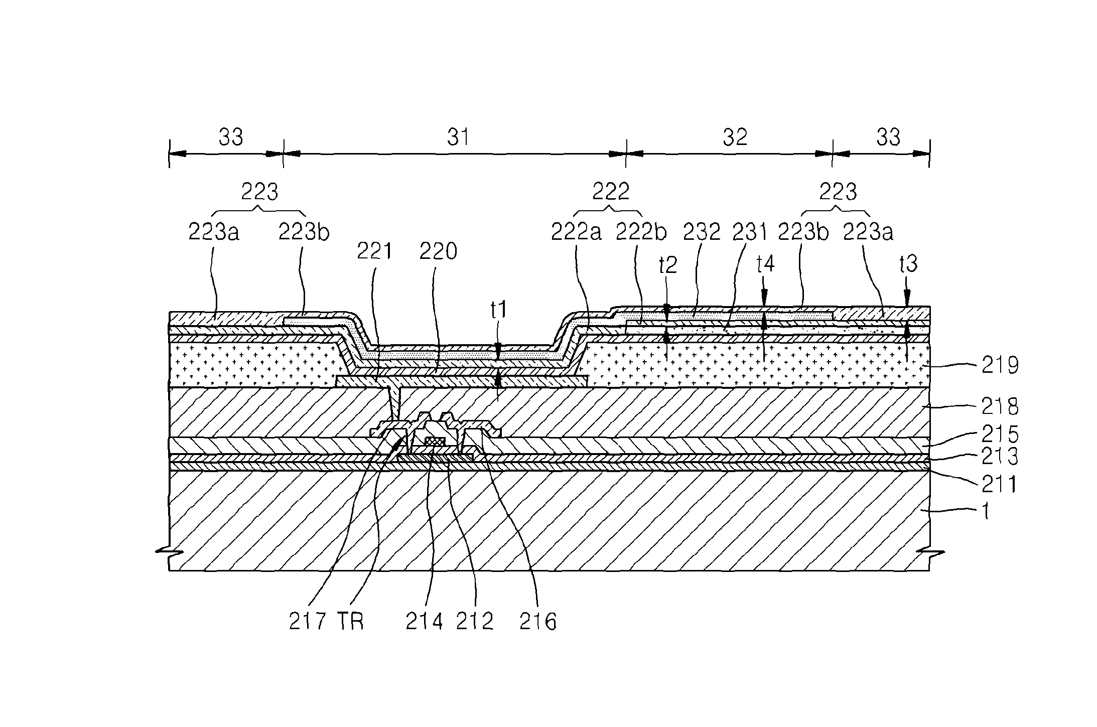
[0042]According to exemplary embodiments of the invention, the second electrode and the third electrode that include metal may be provided by patterning without using a separate patterning mask, a process of providing the second and third electrodes is substantially simplified. In such embodiments, the second electrode and the third electrode expose the second region including the transmission region, and thus, transmittance of the entire panel may be substantially improved.
[0043]In such embodiments, the third electrode may reduce resistance of the second electrode.

Problems solved by technology

When the transparent / translucent metal is used, a large-sized panel may be not be efficiently manufactured due to high sheet resistance of the cathode, and when the opaque metal is used, a fine metal mask, which is typically used in a conventional organic material patterning process to form an opening pattern, may be not be effectively used.

Method used


Image

  • Organic light-emitting display apparatus and manufacturing method thereof
  • Organic light-emitting display apparatus and manufacturing method thereof
  • Organic light-emitting display apparatus and manufacturing method thereof

Examples


Embodiment Construction

[0058]The invention will be described more fully hereinafter with reference to the accompanying drawings, in which embodiments of the invention are shown. This invention may, however, be embodied in many different forms, and should not be construed as limited to the embodiments set forth herein. Rather, these embodiments are provided so that this disclosure will be thorough and complete, and will fully convey the scope of the invention to those skilled in the art. Like reference numerals refer to like elements throughout.

[0059]It will be understood that when an element or layer is referred to as being “on,”“connected to” or “coupled to” another element or layer, the element or layer can be directly on, connected or coupled to the other element or layer or intervening elements or layers may be present. In contrast, when an element is referred to as being “directly on,”“directly connected to” or “directly coupled to” another element or layer, there are no intervening elements or layer...


PUM


Abstract

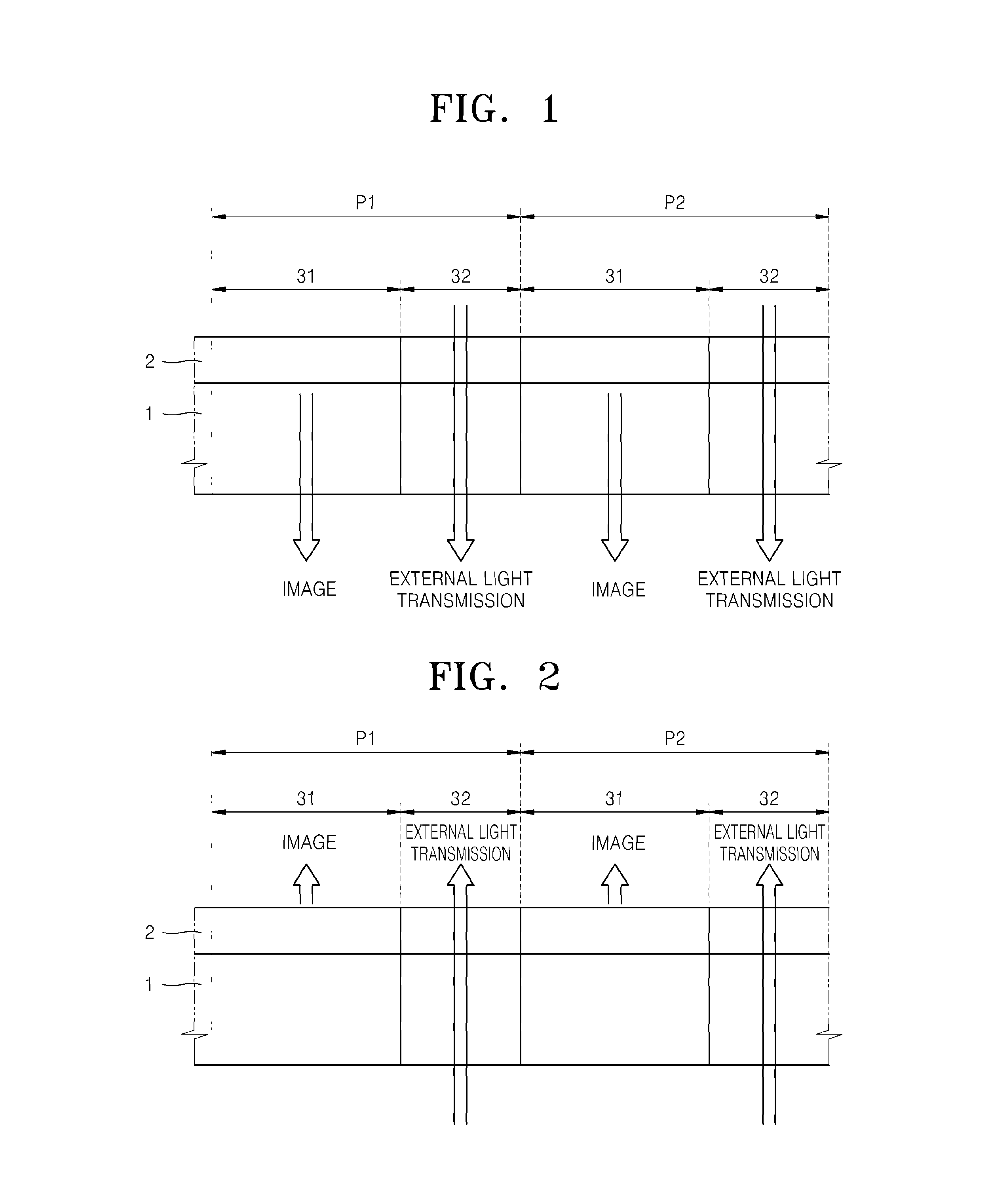
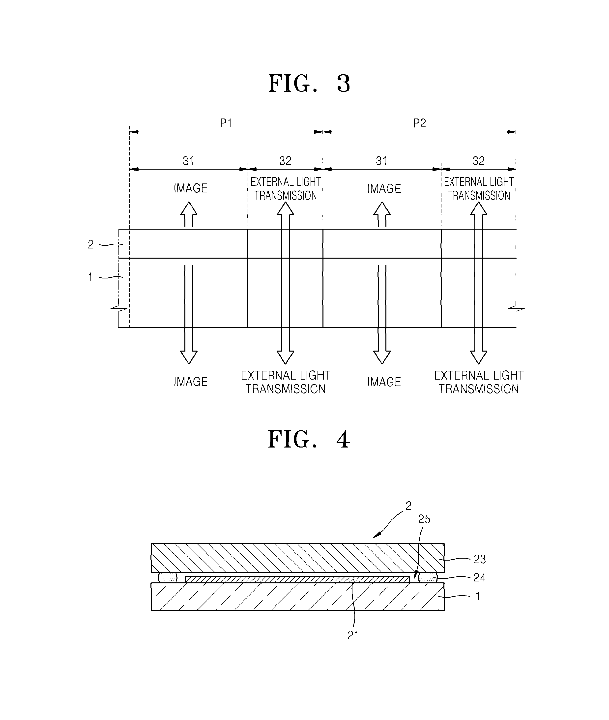
An organic light-emitting display apparatus includes: a substrate; pixels defined on the substrate, where each pixel includes a first region including a light-emitting region and a second region including a transmission region; a third region defined on the substrate disposed between the pixels; first electrodes disposed in the pixels on the substrate, respectively, where each first electrode is disposed in the first region of a corresponding pixel; an organic emission layer disposed to cover the first electrodes; a first auxiliary layer disposed on the organic emission layer in the second region and which exposes the first region; a second electrode disposed on the organic emission layer in the first region; a second auxiliary layer disposed in the first and second regions and which exposes the third region; and a third electrode disposed in the third region and in contact with the second electrode.

Description

[0001]This application claims priority to Korean Patent Application No. 10-2013-0086961, filed on Jul. 23, 2013, and all the benefits accruing therefrom under 35 U.S.C. §119, the content of which in its entirety is herein incorporated by reference.BACKGROUND[0002]1. Field[0003]One or more exemplary embodiments of the invention relate to an organic light-emitting display apparatus and a manufacturing method of the organic light-emitting display apparatus.[0004]2. Description of the Related Art[0005]An organic light-emitting display apparatus is a self light-emitting display that electrically excites an organic compound to emit light. Since the organic light-emitting display apparatus may be operated at a low voltage, may be easily formed in a thin profile, and may have wide viewing angles and fast response speeds, the organic light-emitting display apparatus has received attention as an advanced display that may address limitations in a liquid crystal display device.[0006]The organic...

Claims


Application Information

Patent Timeline
Patent Type & Authority Patents(United States)
IPC IPC(8): H01L29/72H01L51/56H01L51/52
CPCH01L51/5203H01L51/56H10K59/353H10K59/121H10K2102/3031H05B33/10H05B33/26H10K50/805H10K2102/351H10K71/00
Inventor CHUNG, JIN-KOOCHOI, JUN-HOCHO, KWAN-HYUN
Owner SAMSUNG DISPLAY CO LTD
Why Eureka
Try Eureka