

Margin improvement for configurable local clock buffer
a local clock buffer and configurable technology, applied in the field of microelectronic devices, can solve the problems of reducing operating voltage, unpredictable variations in propagation times, and delay in propagation through the devi
- Summary
- Abstract
- Description
- Claims
- Application Information
AI Technical Summary
Problems solved by technology
Method used
Image

Examples
Embodiment Construction
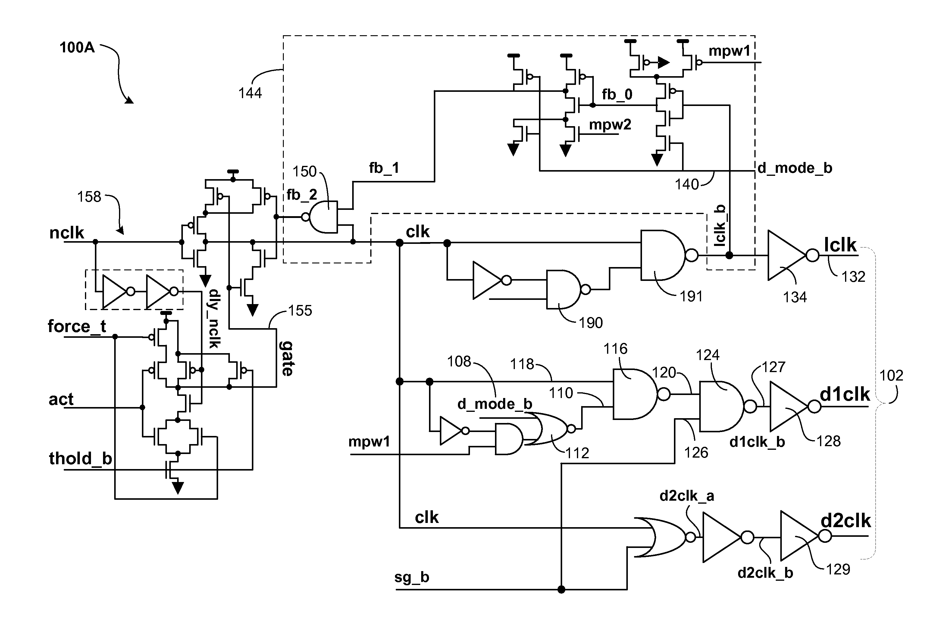
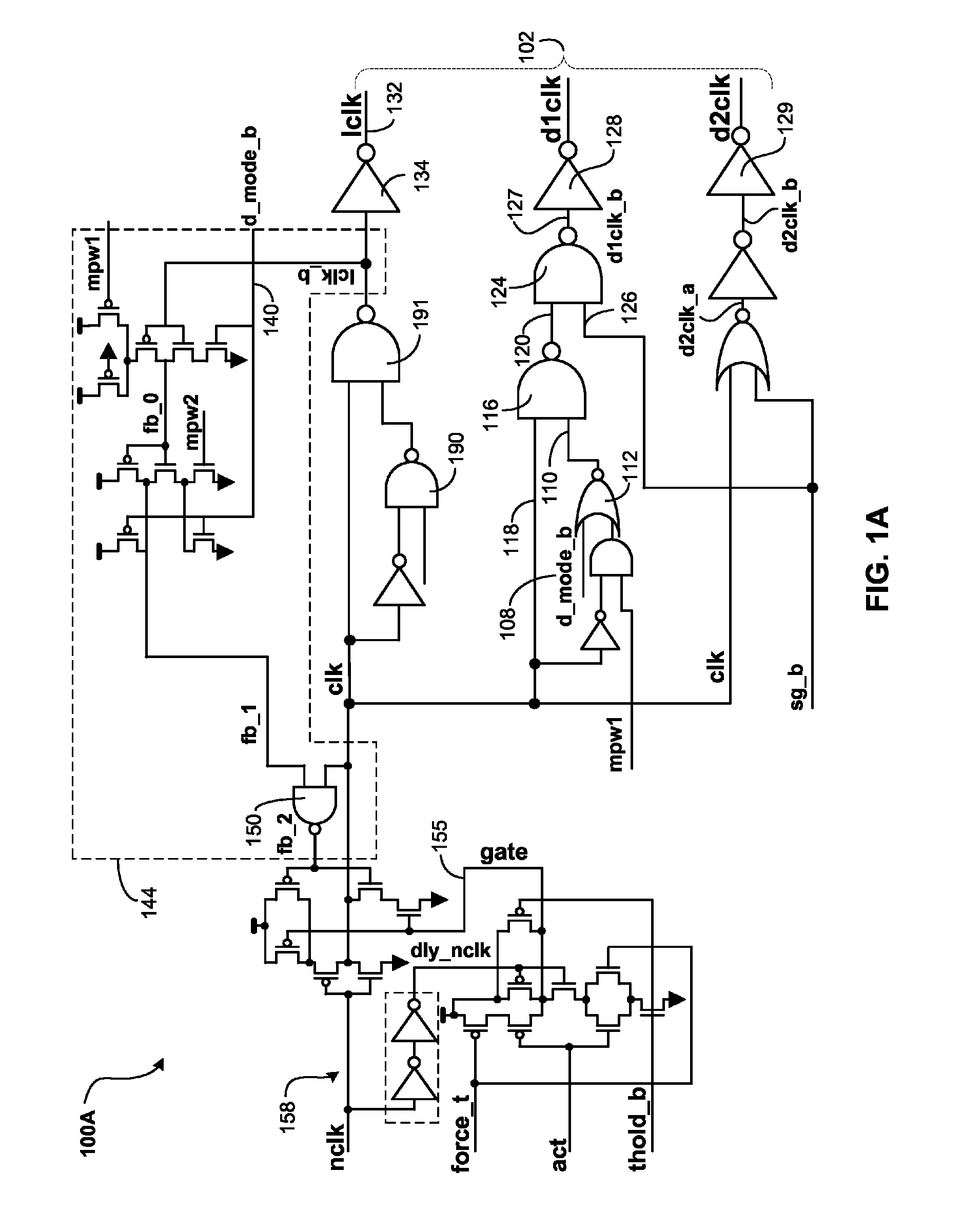
[0015]The following one or more exemplary embodiments describe a local clock buffer circuit that introduces a timing margin into controlling the clock signal in order to avoid race conditions.
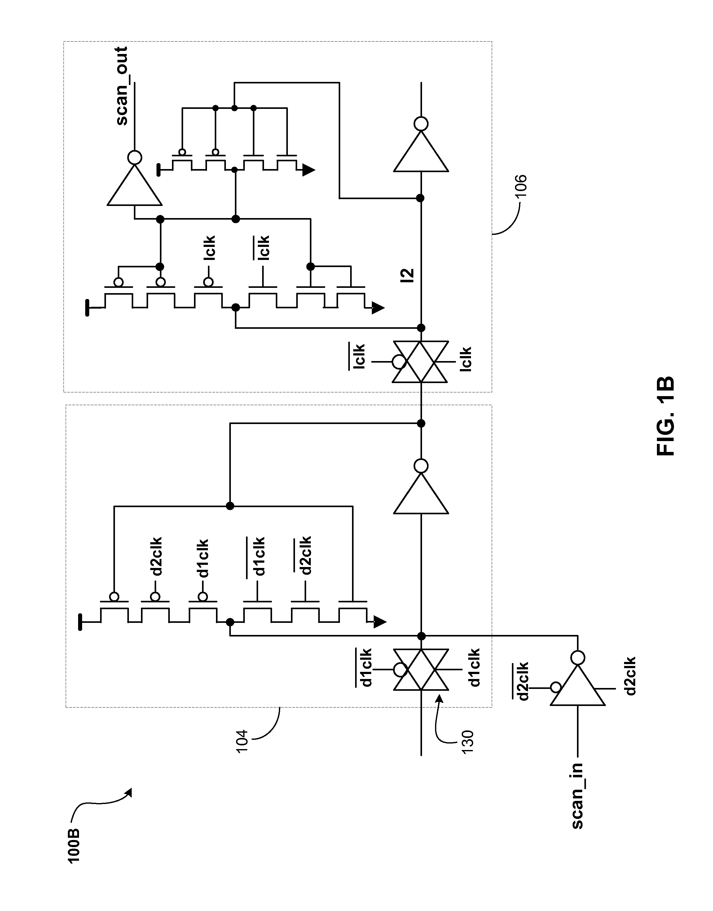
[0016]Referring to FIG. 1A, a local clock buffer circuit 100A may be used to drive sequential devices such as, for example, a plurality of latches (e.g., 30 latches). As depicted in FIG. 1B, the outputs 102 of the local clock buffer circuit 100A are used to drive an exemplary latch circuit 100B including a master latch 104 and a slave latch 106 stage. Specifically, the generated local clock signal lclk, the d1 clock d1clk, and the d2 clock d2clk of the local clock buffer circuit 100A, and their respective complementary signals (i.e., lclk, d1clk, d2clk), are driving latch circuitry 100B.
[0017]Referring to FIG. 1A, the d_mode_b control input 108 may be utilized to place the local clock buffer circuit 100A in either a self-timed pulse operating mode or in a master / slave type operating mode. For e...
PUM
 Abstract
Description
Claims
Application Information