Delay locked loop circuit

a delay line and lock loop technology, applied in the field of delay lock loop circuits, can solve problems such as difficult to secure a sufficient comparison time, reduce the delay of delay lines, and problems such as problems such as problems such as problems such as problems such as problems such as problems such as problems such as problems such as the delay of the delay lin

Active Publication Date: 2008-03-25
SK HYNIX INC
View PDF19 Cites 22 Cited by
  • Summary
  • Abstract
  • Description
  • Claims
  • Application Information

AI Technical Summary

Benefits of technology

[0023]It is, therefore, an object of the present invention to provide a delay locked loop (DLL) circuit of a semiconductor memory device for performing an accurate phase update even if an entry into and an exit from the power down mode are repeated frequently because of a short period of a clock enable signal, and a locking method thereof.
[0024]In accordance with an aspect of the present invention, there is provided a synchronous memory device having a normal mode and a power down mode, including: a delay locked loop (DLL), without performing a phase update operation in the power down mode, for generating a DLL clock having frozen locking information when exiting the power down mode; and a controller for stopping the phase update operation of the DLL when a predetermined time passes after entering the power down mode to thereby obtain a time margin for the phase update operation in the normal mode.

Problems solved by technology

If the clock enable signal CKE has a short period as shown in FIG. 3 and repeats the entry and exit into / from the power down mode frequently, problems may occur, as discussed below.
Second, it is difficult to secure a sufficient comparison time for comparing the internal clock signal REF_CLK and the feedback clock signal FEEDBACK CLOCK with each other if the duration time of a logic level ‘HIGH’ of the clock enable signal CKE is too short.
Since the comparison time is not sufficient, i.e., the internal clock signal REF_CLK is not being toggled when the phases of the internal clock signal REF_CLK and the feedback clock signal FEEDBACK CLOCK are being compared, the result of the phase detector always causes the erroneous operation of ordering to reduce the delay of the delay line.
Due to the foregoing reasons, the determined information for the DLL clock is inaccurate.
As a result, if a bank is activated and a read operation is performed using the output clock of the DLL with the erroneous lock information, the output of the DRAM is distorted in comparison with the external clock so that it is difficult to transmit / receive the data normally.

Method used


Image

  • Delay locked loop circuit
  • Delay locked loop circuit
  • Delay locked loop circuit

Examples


Embodiment Construction

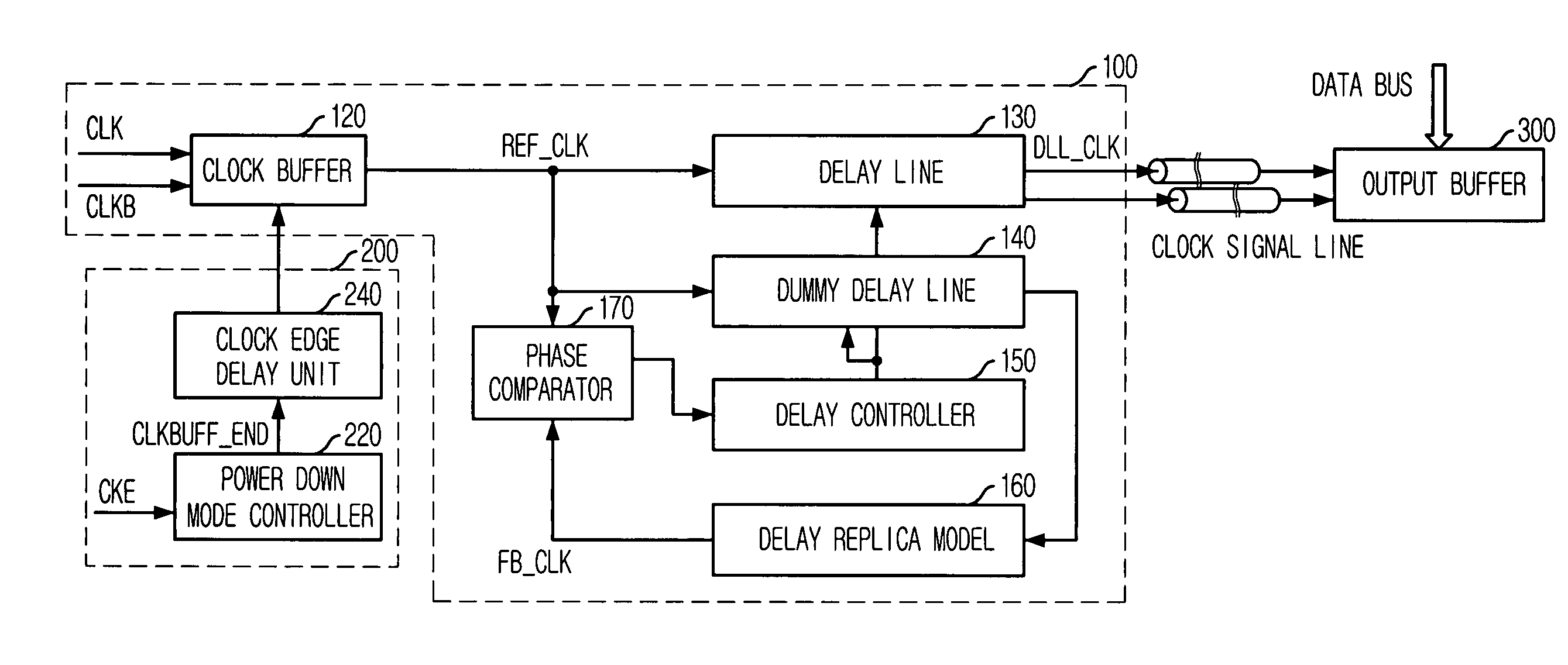
[0038]A delay locked loop (DLL) circuit in accordance with exemplary embodiments of the present invention will be described in detail with reference to the accompanying drawings.

[0039]FIG. 4 is a block diagram illustrating a DLL circuit in accordance with an embodiment of the present invention.

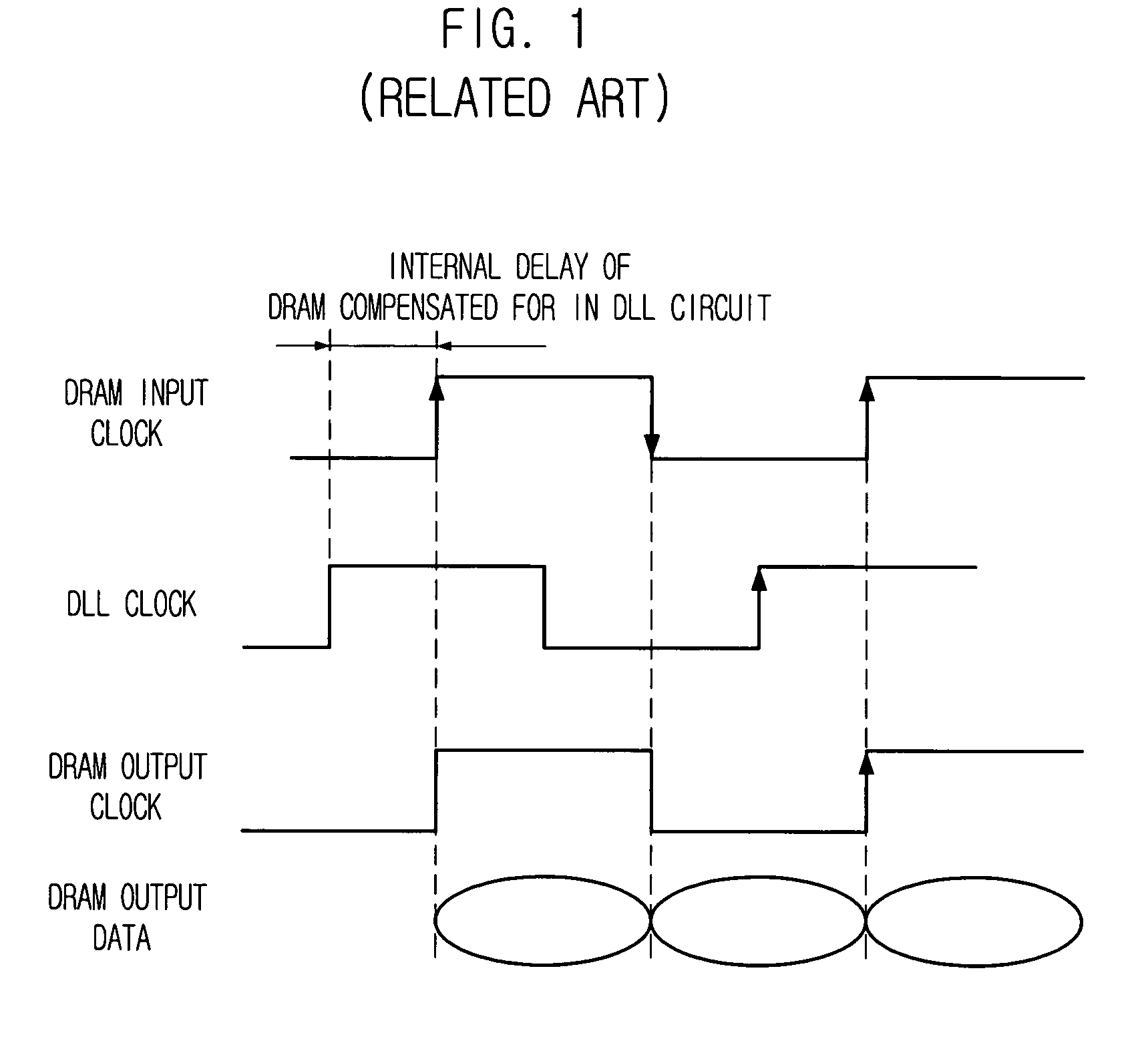
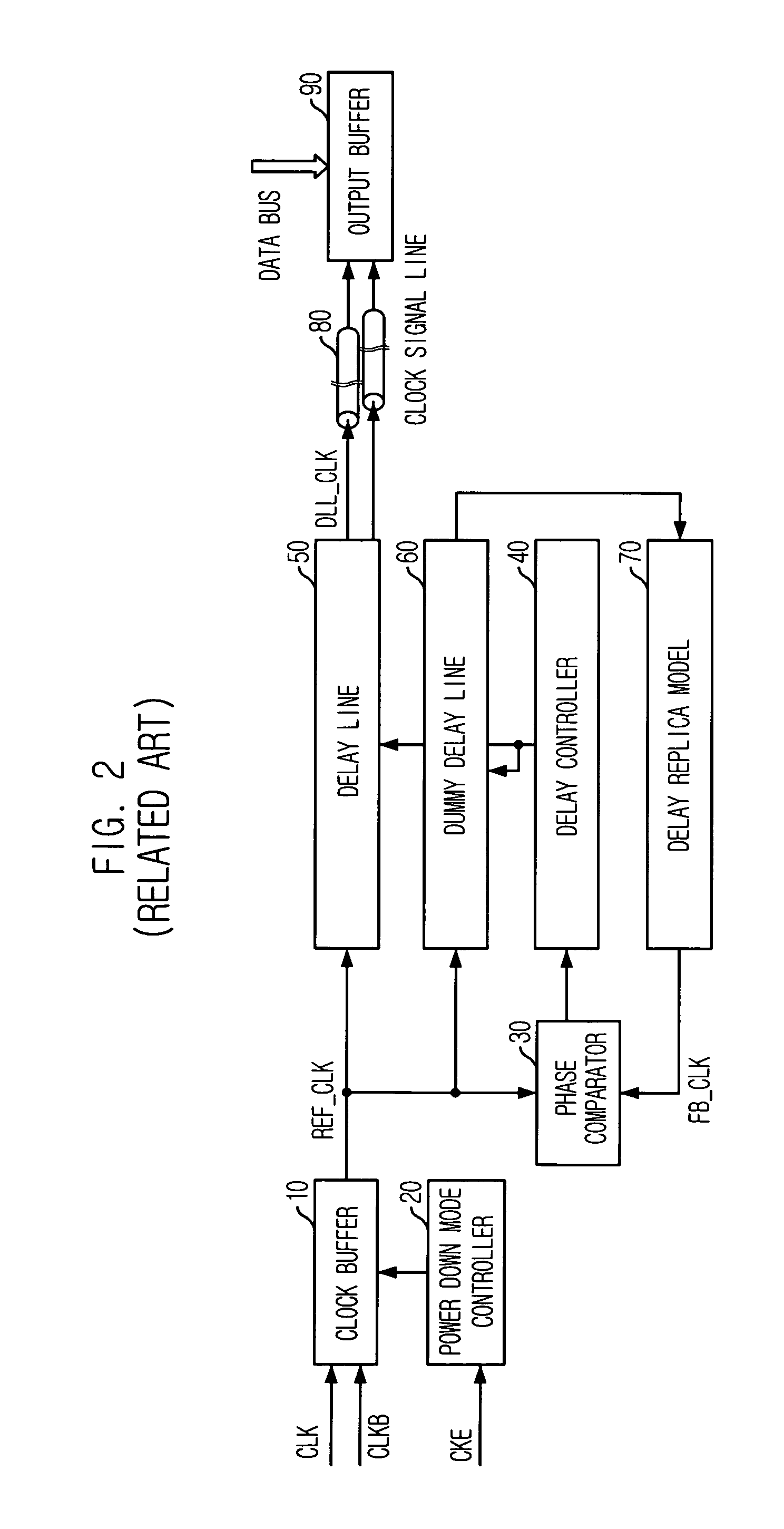
[0040]The DLL circuit in accordance with the embodiment of the present invention which is employed in a synchronous memory device having a normal mode and a power down mode for low power consumption, includes a DLL 100 and a controller 200. The DLL 100 does not perform a phase update in the power down mode and generates a DLL clock having frozen locking information when exiting the power down mode. The controller 200 stops performing the phase update operation of the DLL when a predetermined time passes after entering the power down mode, to obtain a time margin for the phase update in the normal mode.

[0041]The controller 200 is configured with a power down mode controller 220 and a clock edge...


PUM


Abstract

A DLL circuit and a synchronous memory device perform stable operation in a power down mode although the entry and exit into / from the power down mode is repeated rapidly. The synchronous memory device operates in a normal mode and a power down mode. A delay locked loop (DLL) generates a DLL clock having frozen locking information when exiting the power down mode. A controller precludes phase update operation of the DLL when a predetermined time passes after entering the power down mode to thereby obtain a time margin for a phase update operation undertaken in the normal mode.

Description

FIELD OF THE INVENTION[0001]The present invention relates to a delay locked loop (DLL) circuit of a synchronous DRAM; and, more particularly, to a DLL circuit for performing a stable operation in a power down mode for low power operation of a semiconductor device.DESCRIPTION OF RELATED ARTS[0002]A synchronous semiconductor memory device such as a double data rate synchronous DRAM (DDR SDRAM) performs data transmission with external devices using an internal clock signal locked in synchronization with an external clock signal inputted from an external device such as a memory controller. Time synchronization between a reference clock signal and data is important for stably transmitting the data between a memory device and a memory controller. In order to transmit the data stably, the data should be positioned accurately at an edge or a center of the clock by compensating for delay time which occurs inevitably by virtue of the time difference between the data transmission of each eleme...

Claims


Application Information

Patent Timeline
Patent Type & Authority Patents(United States)
IPC IPC(8): H03L7/06
CPCG11C7/1072G11C7/222H03L7/0805H03L7/0814H03L7/0816
Inventor CHOI, HOON
Owner SK HYNIX INC
Why Eureka
Try Eureka