Supercharge Your Innovation With Domain-Expert AI Agents!

Adaptive sampling for semiconductor inspection recipe creation, defect review, and metrology

Active Publication Date: 2015-08-04
KLA CORP
View PDF11 Cites 26 Cited by
  • Summary
  • Abstract
  • Description
  • Claims
  • Application Information

AI Technical Summary

Benefits of technology

This patent describes a computer-implemented method and system for adaptive sampling for wafers. The method involves scanning the wafer with a first tool (which is faster and has lower resolution) to generate first images, and then using an unsupervised clustering algorithm to separate the segments from the first images. A second tool (which is slower and has higher resolution) is used to acquire second images for the sample of segments. The characteristics of the segments are determined based on the second images and associated with all the segments in a specific group. This method allows for better selection of relevant segments and improved accuracy in identifying characteristics of the wafer.

Problems solved by technology

In addition, the method includes clustering the feature vectors using an unsupervised clustering algorithm thereby separating the segments into different groups based on the feature vectors and selecting one or more of the segments from a first of the different groups thereby creating a sample of segments for the first of the different groups.

Method used


Image

  • Adaptive sampling for semiconductor inspection recipe creation, defect review, and metrology
  • Adaptive sampling for semiconductor inspection recipe creation, defect review, and metrology
  • Adaptive sampling for semiconductor inspection recipe creation, defect review, and metrology

Examples


Embodiment Construction

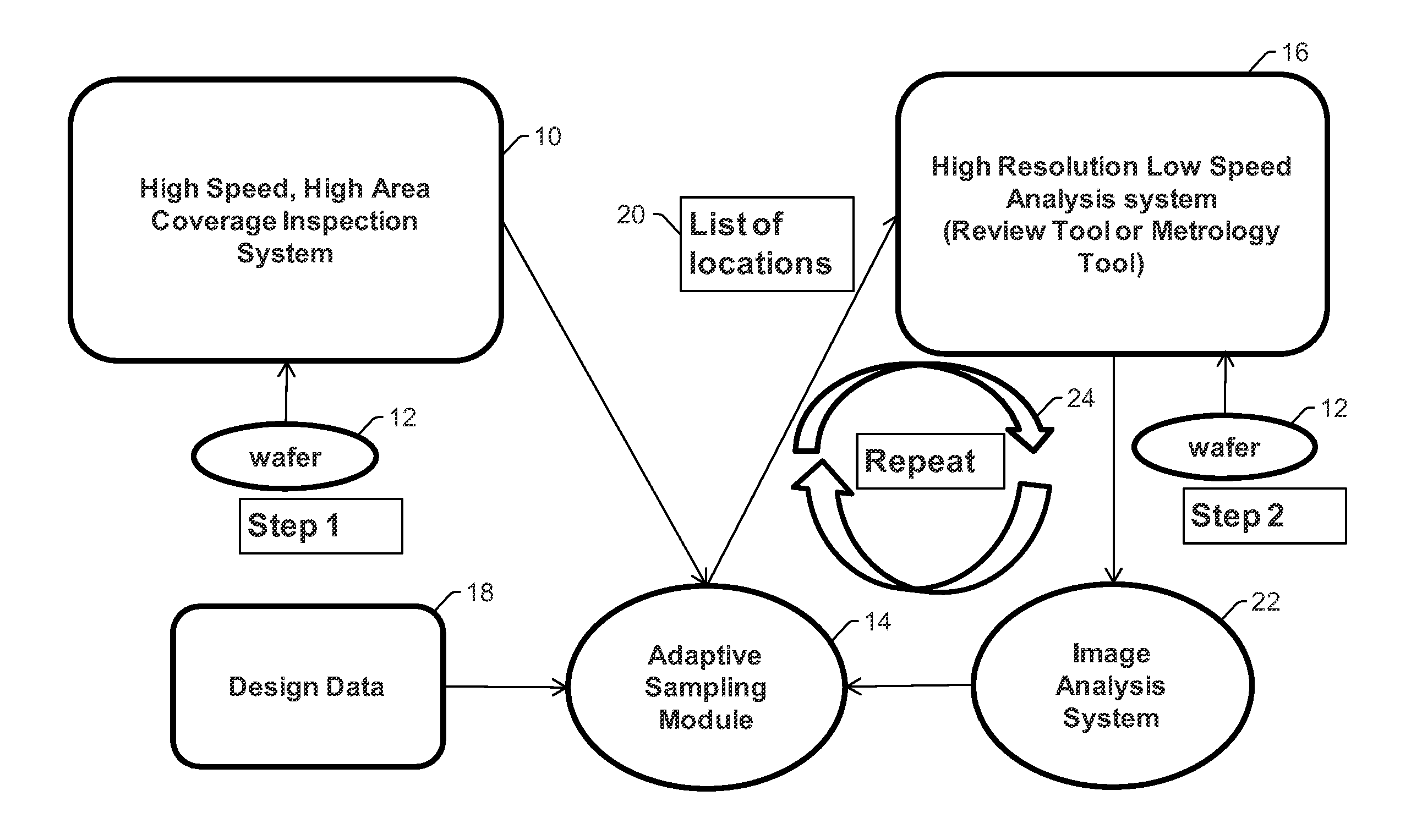
[0020]Turning now to the drawings, it is noted that the figures are not drawn to scale. In particular, the scale of some of the elements of the figures is greatly exaggerated to emphasize characteristics of the elements. It is also noted that the figures are not drawn to the same scale. Elements shown in more than one figure that may be similarly configured have been indicated using the same reference numerals. Unless otherwise noted herein, any of the elements described and shown may include any suitable commercially available elements.

[0021]One embodiment relates to a computer-implemented method for adaptive sampling. The method includes scanning at least a portion of a wafer with a first tool thereby generating one or more first images of at least the portion of the wafer. Scanning at least the portion of the wafer may be performed in any suitable manner. For example, the first tool may scan the wafer in a serpentine manner and generate images as the wafer is being scanned. The f...


PUM


Abstract

Methods and systems for adaptive sampling for semiconductor inspection recipe creation, defect review, and metrology are provided. The embodiments provide image processing and pattern recognition algorithms and an adaptive sampling method for extracting critical areas from SEM image patches for use in a wafer inspection system when design data for a semiconductor chip is not available. The embodiments also provide image processing and pattern recognition algorithms for efficiently discovering critical defects and significant deviations in the normal manufacturing process, using the output from a wafer inspection system and an adaptive sampling method to select wafer locations to be examined on a high resolution review or metrology tool.

Description

BACKGROUND OF THE INVENTION[0001]1. Field of the Invention[0002]This invention generally relates to adaptive sampling for semiconductor inspection recipe creation, defect review, and metrology.[0003]2. Description of the Related Art[0004]The following description and examples are not admitted to be prior art by virtue of their inclusion in this section.[0005]Semiconductor manufacturing involves a large and complex set of imaging, etching, deposition, and planarization processes in order to construct sub-micron (down to a few tens of nanometers) geometrical patterns on a silicon substrate. The usual method for detecting most random and low probability systematic defects is to compare identical locations on adjacent dies on the wafer using imaging or scattering optical tool such as the KLA-Tencor 2900 Series or KLA-Tencor 9800 Series systems. However, this task is becoming more challenging as the process windows of tolerance become tighter. Tool noise (such as sensor noise and image m...

Claims


Application Information

Patent Timeline
Patent Type & Authority Patents(United States)
IPC IPC(8): G06K9/00G06T7/00
CPCG06T7/0004G06T2207/30148G06T2207/10061
Inventor KULKARNI, ASHOK V.BANERJEE, SAIBAL
Owner KLA CORP
Features
  • R&D
  • Intellectual Property
  • Life Sciences
  • Materials
  • Tech Scout
  • Unparalleled Data Quality
  • Higher Quality Content
  • 60% Fewer Hallucinations
Learn More