
Electric power converter and method of manufacturing the same

a technology of electric power converter and assembly method, which is applied in the direction of electrical apparatus, semiconductor devices, semiconductor/solid-state device details, etc., can solve the problems of contaminating the pressure applied to the semiconductor stacking unit may not be uniform, etc., and achieves the effect of improving the assembly performance of the electric power converter, and being easy to attach

Inactive Publication Date: 2015-08-11
TOYOTA JIDOSHA KK
View PDF11 Cites 1 Cited by
  • Summary
  • Abstract
  • Description
  • Claims
  • Application Information

AI Technical Summary

Benefits of technology

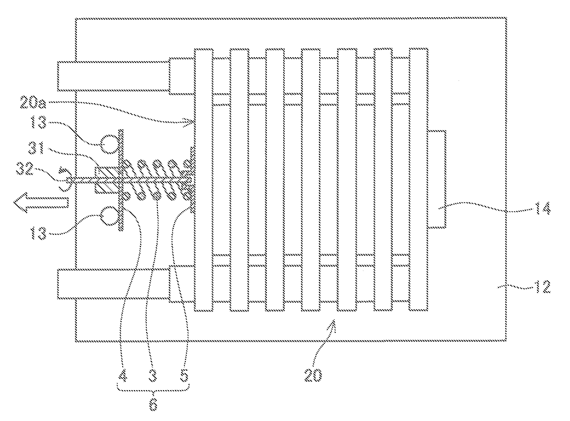
[0011]In the novel electric power converter disclosed in the present specification, the spring unit having the penetrating passage which is open to the bottom of the recess of the first plate improves the assembly performance of the electric power converter. The lock pin which is passed through from the second plate side compresses the spring, and the hook at the tip of the lock pin engages the first plate. The lock pin easily causes the spring unit to be in the compressed state. The tip of the lock pin that includes the hook is disposed in the recess of the first plate. Therefore, the first plate can make contact with the end surface of the semiconductor stacking unit without the tip of the lock pin interfering. When the lock pin is disengaged, the first plate applies pressure uniformly to the semiconductor stacking unit. Further, unlike the bolt of Patent Document 3, the lock pin having the hook on the tip does not require a screw hole, and does not generate dust. The technique described above improves the assembly performance of the electric power converter.

Problems solved by technology

For example, since the rear side plate of the spring unit is rotated while the spring unit is being pressed against the semiconductor stacking unit in the technique of Patent Document 2, twisting force may possibly be applied to the semiconductor stacking unit, and that while the rear side plate is being rotated and after the compression of the spring unit, the pressure applied to the semiconductor stacking unit may not be uniform.
Further, since a bolt is used in the technique of Patent Document 3, dust may possibly be generated when the bolt is disengaged from the screw hole, thus contaminating the semiconductor stacking unit.

Method used


Image

  • Electric power converter and method of manufacturing the same
  • Electric power converter and method of manufacturing the same
  • Electric power converter and method of manufacturing the same

Examples


Embodiment Construction

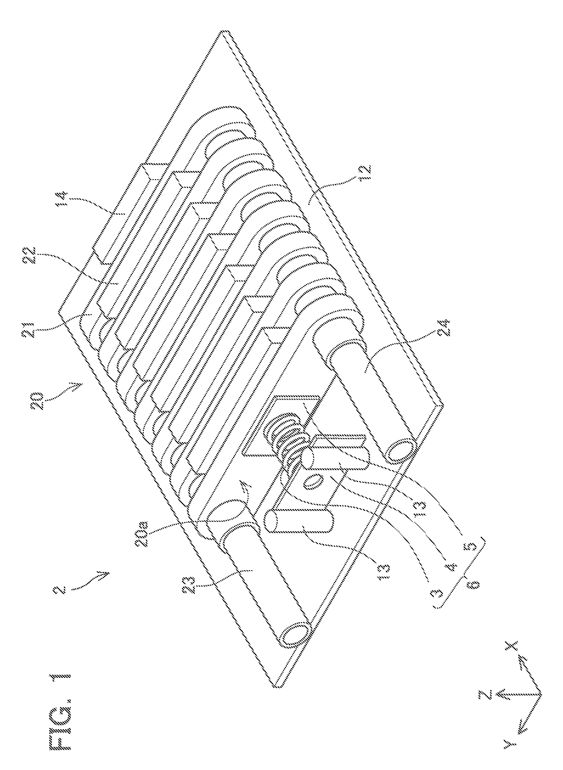
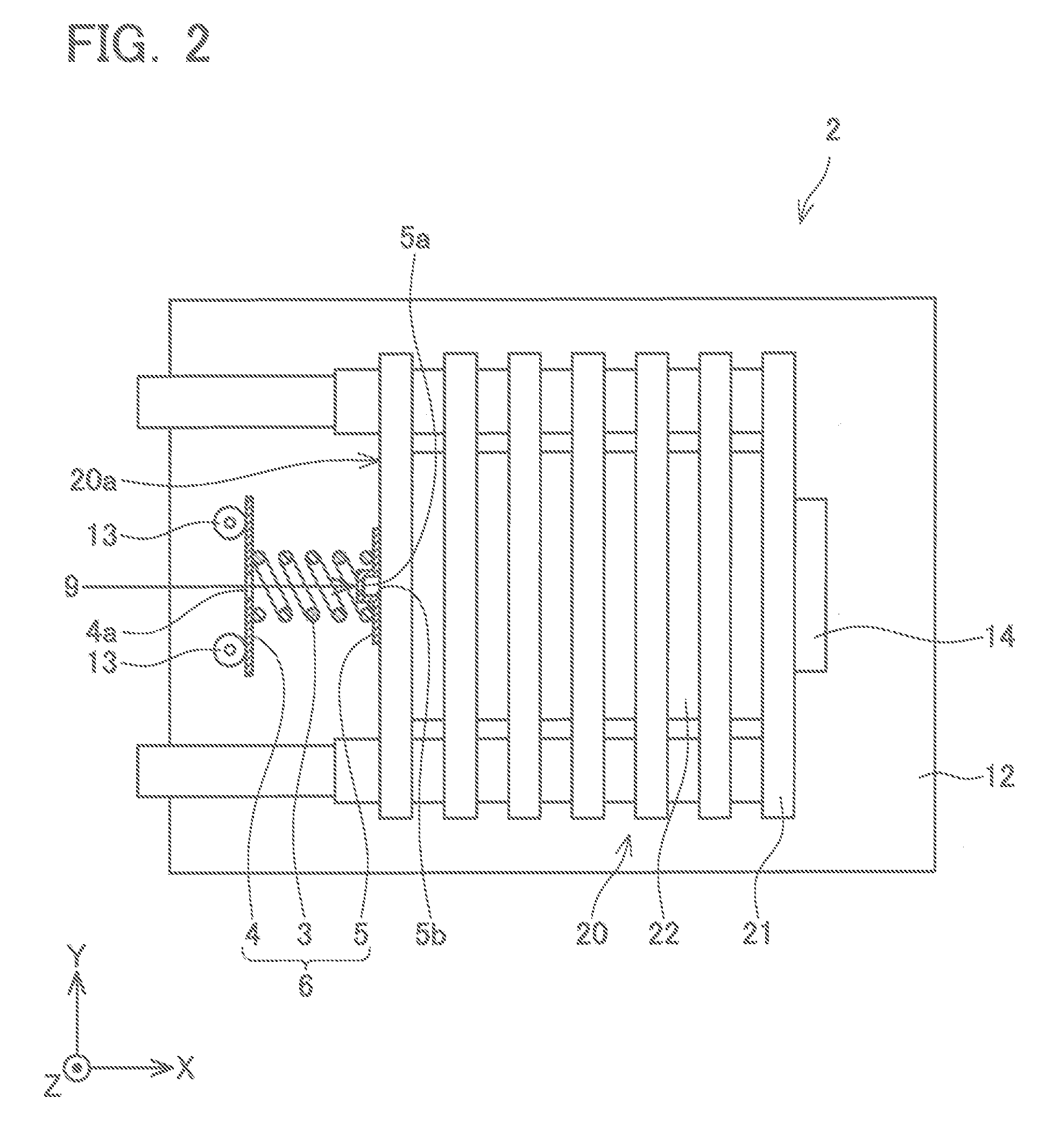
[0023]An electric power converter of the embodiment will be described with reference to the drawings. The electric power converter of the embodiment is an inverter that supplies AC power to a motor. FIG. 1 shows a perspective view of an inverter 2. Moreover, in addition to a semiconductor stacking unit 20 in which power semiconductor elements such as IGBTs or diodes which are used in a switching circuit are stacked, the inverter 2 has a circuit for generating a PWM for driving the power semiconductor element, a circuit for smoothing current, a housing etc., but illustration and description thereof will be omitted.

[0024]Since power semiconductor elements create a large amount of heat, the power semiconductor elements are integrated separately from other circuit components, and are cooled intensively. The inverter 2 utilizes a plurality of power semiconductor elements. The plurality of power semiconductor elements is packaged such that several power semiconductor elements am each in a...


PUM


Abstract

An electric power converter that can easily be assembled is provided. An electric power converter includes a semiconductor stacking unit, a frame and a spring unit. The semiconductor stacking unit has a configuration in which the semiconductor modules and coolers are stacked. The spring unit is inserted between one end of the semiconductor stacking unit in a stacking direction, and a support provided on the frame, and fixes the semiconductor stacking unit while applying pressure thereto. The spring unit is provided with a first plate, a second plate, and a coil spring sandwiched between the first and second plates. A recess is provided in the first plate so as to have a gap between the first plate and the end surface of the semiconductor stacking unit. A penetrating passage through which the entire spring unit passes along a bottom of the recess is provided in the spring unit.

Description

TECHNICAL FIELD[0001]The technique disclosed in the present specification relates to an electric power converter such as an inverter or converter, and a method of manufacturing the same.BACKGROUND ART[0002]In an inverter which supplies power to a motor or in a voltage converter which converts voltage, a structure may be adopted in which a semiconductor element which generates a large amount of heat, such as an IGBT, is integrated separately from other circuits, and is cooled intensively. In one such integrated structure, a semiconductor stacking unit is known in which a flat type semiconductor module for containing a semiconductor element, and a flat type cooler are stacked alternately (e.g., Patent Document 1 to Patent Document 3).[0003]In order to transfer heat well from the semiconductor module to the cooler, the semiconductor stacking unit is placed on a frame while pressure is being applied to the semiconductor stacking unit in a stacking direction. Here, the frame is a structu...

Claims


Application Information

Patent Timeline
Patent Type & Authority Patents(United States)
IPC IPC(8): H01L23/367H01L23/40H01L21/52
CPCH02M7/003H01L21/52H01L23/367H01L23/3675H01L23/40H01L2924/0002H01L2924/00
Inventor HIRONAKA, RYOUJIIMURA, HITOSHI
Owner TOYOTA JIDOSHA KK
Learn More