Stack bank type semiconductor memory apparatus capable of improving alignment margin

a semiconductor memory and alignment margin technology, applied in static storage, digital storage, instruments, etc., can solve the problems of insufficient alignment margin between the banks, insufficient gap between the sub-banks, and reduced line width, so as to improve the alignment margin of the bank

Active Publication Date: 2015-09-01
SK HYNIX INC
View PDF25 Cites 8 Cited by
  • Summary
  • Abstract
  • Description
  • Claims
  • Application Information

AI Technical Summary

Benefits of technology

[0014]A semiconductor memory apparatus capable of improving the alignment margin for a bank is described herein. A semiconductor memory apparatus capable of sufficiently ensuring a space for forming a global input / output line is also described herein.

Problems solved by technology

Therefore, the alignment margin between the banks 12 is insufficient, and a sufficient gap between the sub-banks 15 may not be sufficiently ensured.
The reduction in the spacing related to the global input / output line causes crosstalk, and the reduction in the line width of the global input / output line causes a signal delay.

Method used


Image

  • Stack bank type semiconductor memory apparatus capable of improving alignment margin
  • Stack bank type semiconductor memory apparatus capable of improving alignment margin
  • Stack bank type semiconductor memory apparatus capable of improving alignment margin

Examples


Embodiment Construction

.”

BRIEF DESCRIPTION OF THE DRAWINGS

[0022]The above and other aspects, features and other advantages of the subject matter of the present disclosure will be more clearly understood from the following detailed description taken in conjunction with the accompanying drawings, in which:

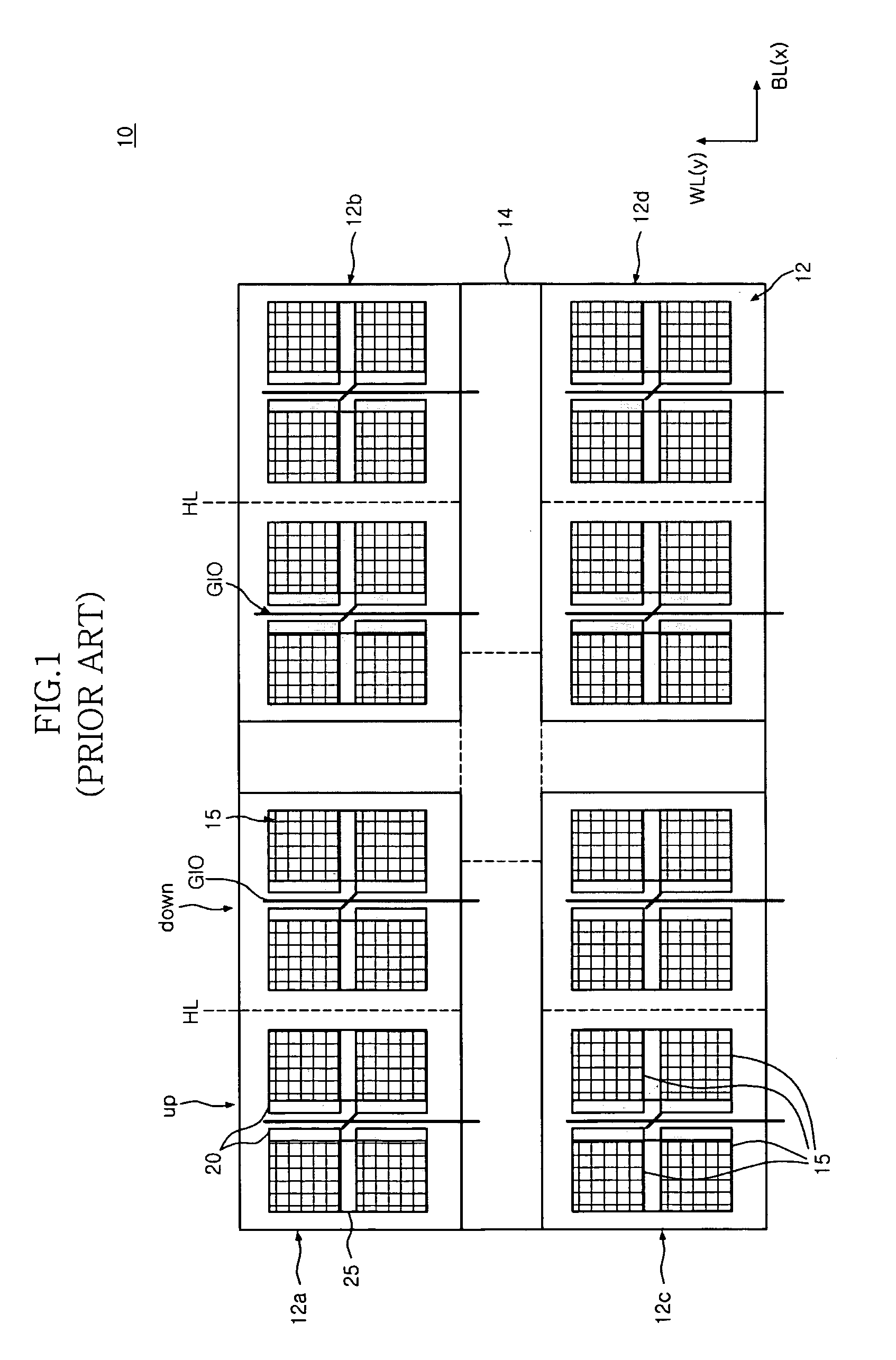
[0023]FIG. 1 is a plan view illustrating a conventional semiconductor memory apparatus employing a multi-bank scheme;

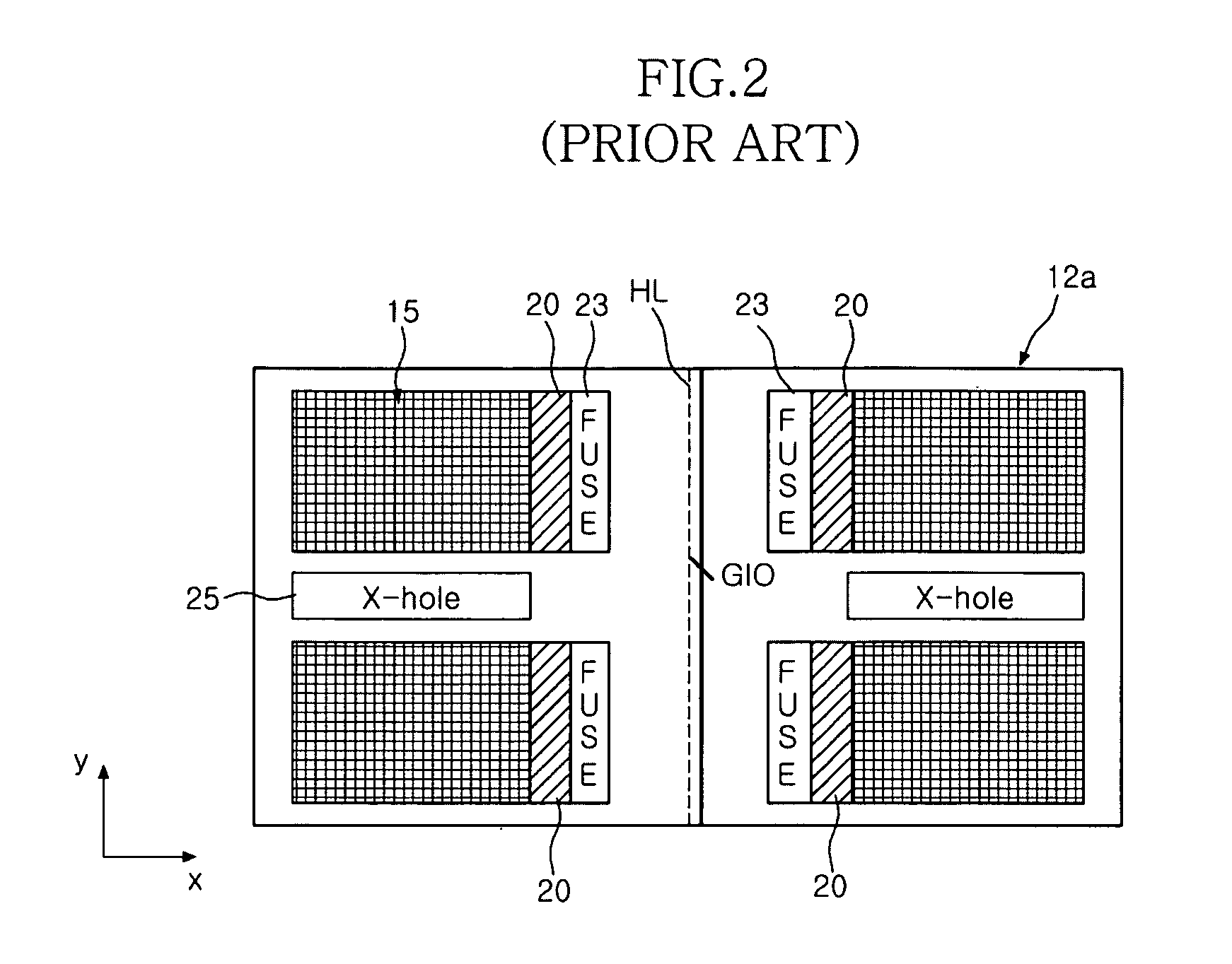
[0024]FIG. 2 is an enlarged plan view illustrating one bank of the semiconductor memory apparatus shown in FIG. 1;

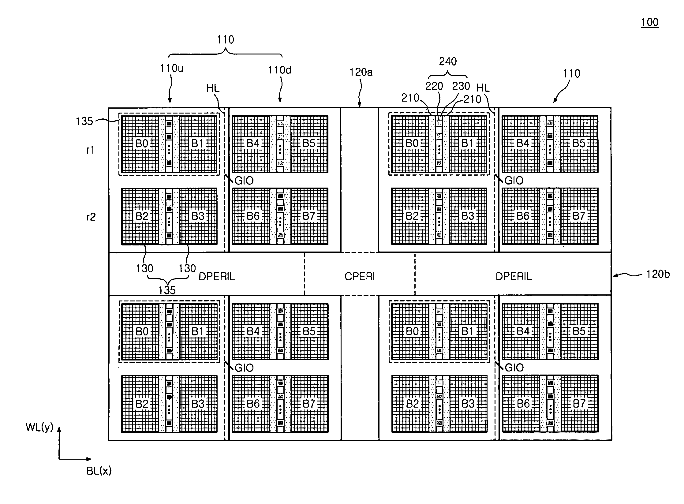
[0025]FIG. 3 is a plan view illustrating a stack bank type semiconductor memory apparatus according to one embodiment;

[0026]FIG. 4 is an enlarged plan view illustrating one stack bank of the semiconductor memory apparatus shown in FIG. 3 according to one embodiment;

[0027]FIG. 5 is an enlarged plan view illustrating one stack bank of the semiconductor memory apparatus shown in FIG. 3 according to another embodiment;

[0028]FIG. 6 is a plan view illustrating a stack bank type semicon...


PUM


Abstract

A semiconductor memory apparatus is capable of improving the alignment margin for a bank and sufficiently ensuring a space for forming a global input / output line. The semiconductor memory apparatus includes a stack bank structure having at least two sub-banks continuously stacked without disconnection of data signal lines, and a control block arranged at one side of the stack bank structure to simultaneously control column-related signals of the sub-banks.

Description

CROSS-REFERENCES TO RELATED APPLICATION[0001]The present application claims priority under 35 U.S.C. 119(a) to Korean application numbers 10-2007-0114146 filed on Nov. 9, 2007, 10-2007-0114944 filed on Nov. 12, 2007 and 10-2007-0115462 filed on Nov. 13, 2007 in the Korean Intellectual Property office, each of which is incorporated by reference in its entirety as if set forth in full.BACKGROUND[0002]1. Technical Field[0003]The embodiments described herein relate to a stack bank type semiconductor memory apparatus, and more particularly, to a semiconductor memory including a plurality of banks having a plurality of sub-banks.[0004]2. Related Art[0005]A conventional semiconductor memory apparatus includes a plurality of memory cells and a circuit for controlling the memory cells. At present, a bank concept has been introduced to control a plurality of memory cells by classifying the memory cells into groups. A bank represents an area that includes a plurality of memory cells. The memor...

Claims


Application Information

Patent Timeline
Patent Type & Authority Patents(United States)
IPC IPC(8): G11C5/02G11C5/06
CPCG11C5/063G11C5/025G11C5/02G11C7/10G11C8/10
Inventor KWAK, SEUNG-WOOKSHIN, SANG-HOONSONG, KEUN-SOO
Owner SK HYNIX INC
Why Eureka
Try Eureka