Method of manufacturing semiconductor device including forming trench pattern in a mask film

a mask film and semiconductor technology, applied in the direction of semiconductor/solid-state device manufacturing, basic electric elements, electric devices, etc., can solve the problems of low dielectric constant film damage, increase in the dielectric constant of low dielectric constant film, and difficulty in sufficiently secure etching selectivity between mask film adjacent to each other, so as to achieve high interconnect reliability and suppress damage

Inactive Publication Date: 2015-09-01
RENESAS ELECTRONICS CORP
View PDF30 Cites 3 Cited by
  • Summary
  • Abstract
  • Description
  • Claims
  • Application Information

AI Technical Summary

Benefits of technology

[0014]According to the embodiment, it is possible to provide a method of manufacturing a semiconductor device which is capable of realizing high interconnect reliability while suppressing damage due to an asking process.

Problems solved by technology

However, the exposure of the low dielectric constant film when a photoresist at the time of patterning the hard mask is removed by an ashing process may cause a concern of the low dielectric constant film being damaged.
In this case, a problem such as an increase in the dielectric constant of the low dielectric constant film occurs.
However, in such a hard mask, it has been difficult to sufficiently secure etching selectivity between mask films adjacent to each other.
In this case, when a trench pattern or a via pattern is formed, there is a concern that defective patterning may occur.
In this case, a reduction in the reliability of an interconnect being formed is caused.

Method used


Image

  • Method of manufacturing semiconductor device including forming trench pattern in a mask film
  • Method of manufacturing semiconductor device including forming trench pattern in a mask film
  • Method of manufacturing semiconductor device including forming trench pattern in a mask film

Examples


first embodiment

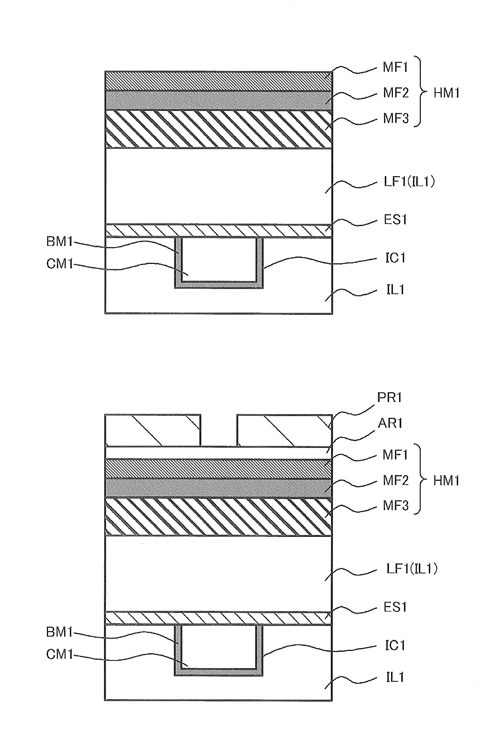
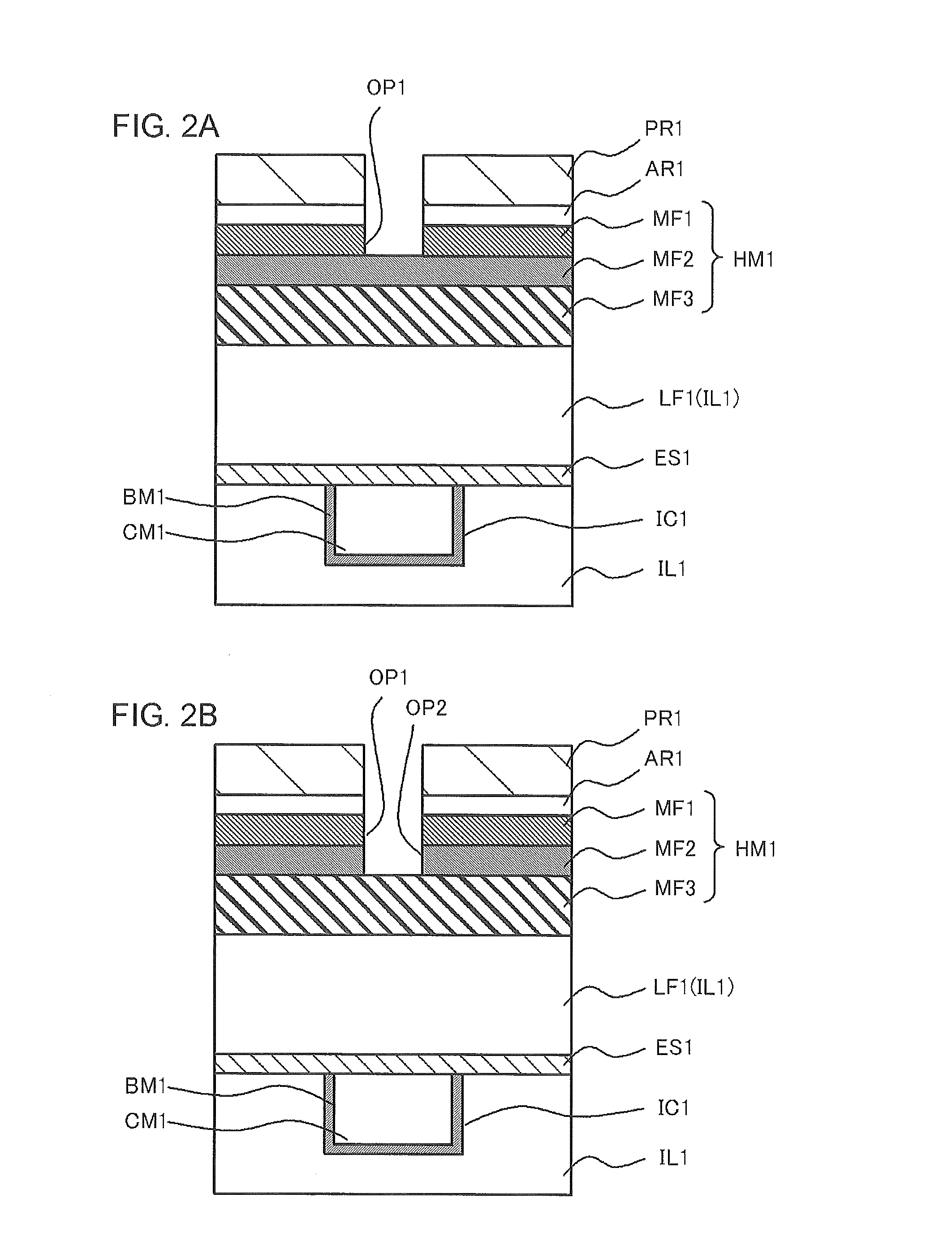
[0038]FIGS. 1A and 1B to FIGS. 7A and 7B are cross-sectional views illustrating a method of manufacturing a semiconductor device SM1 according to a first embodiment. The method of manufacturing the semiconductor device SM1 according to the present embodiment is performed as follows.

[0039]First, a hard mask film HM1 having at least three layers is formed on a low dielectric constant film having a lower dielectric constant than that of a silicon oxide. Here, the hard mask film HM1 formed of an insulating material and the hard mask film HM1 formed of a metal material, amorphous silicon or polycrystalline silicon are alternately laminated.

[0040]Next, etching of the hard mask film HM1 using a photoresist as a mask and an aching process of removing the photoresist are repeated. Thereby, a trench pattern is formed in a first mask film MF1 constituting the hard mask film HM1 which is located at an uppermost layer. In addition, a via pattern located on the inside of the trench pattern, when ...

second embodiment

[0118]FIGS. 9A and 9B to FIGS. 15A and 15B are cross-sectional views illustrating a method of manufacturing a semiconductor device SM1 according to a second embodiment, and correspond to FIGS. 1A and 1B to FIGS. 7A and 7B in the first embodiment.

[0119]In the method of manufacturing the semiconductor device SM1 according to the present embodiment, a process of forming each interconnect layer WL1 is performed using a hard mask film HM1 having four layers. Except for this point, the method of manufacturing the semiconductor device SM1 according to the present embodiment is the same as that in first embodiment.

[0120]Hereinafter, a method of forming each interconnect layer WL1 according to the present embodiment will be described.

[0121]First, as shown in FIG. 9A, the etching stopper film ES1 and the low dielectric constant film LF1 are formed in order on the insulating interlayer IL1 in which the interconnect IC1 is buried. The configurations of the low dielectric constant film LF1 and t...

third embodiment

[0166]FIGS. 16A and 16B to FIGS. 20A and 20B are cross-sectional views illustrating a method of manufacturing a semiconductor device SM1 according to a third embodiment, and correspond to FIGS. 1A and 1B to FIGS. 7A and 7B in the first embodiment.

[0167]In the method of manufacturing the semiconductor device SM1 according to the present embodiment, a process of forming each interconnect layer WL1 is performed using a hard mask film HM1 having five layers. In addition, after a trench pattern is formed in the hard mask film HM1, a via pattern is formed. Meanwhile, the configuration of the semiconductor device SM1 according to the present embodiment is the same as that of the first embodiment.

[0168]Hereinafter, a method of forming each interconnect layer WL1 according to the present embodiment will be described.

[0169]First, as shown in FIG. 16A, the etching stopper film ES1 and the low dielectric constant film LF1 are formed in order on the insulating interlayer IL1 in which the interco...


PUM

PropertyMeasurementUnit
dielectric constantaaaaaaaaaa
thicknessaaaaaaaaaa
thicknessaaaaaaaaaa

Abstract

Provided is a method of manufacturing a semiconductor device in which a via hole and a trench are formed in a low dielectric constant film using a hard mask film having at least three layers. In a process of forming the hard mask film having at least three layers, the hard mask film formed of an insulating material and the hard mask film formed of a metal material, amorphous silicon or polycrystalline silicon are alternately laminated.

Description

[0001]This application is based on Japanese patent application No. 2012-230525, the content of which is incorporated hereinto by reference.BACKGROUND[0002]1. Technical Field[0003]The invention relates to a method of manufacturing a semiconductor device, and relates to, for example, a technique applicable to a method of manufacturing a semiconductor device including an etching process using a hard mask.[0004]2. Related Art[0005]In methods of manufacturing a semiconductor device, an interconnect layer may be formed by, for example, etching using a hard mask. In this manner, techniques including a process of forming an interconnect layer by etching using a hard mask include, for example, techniques disclosed in Japanese Unexamined Patent Publication No. 2003-100871, Pamphlet of International Publication No. WO2007 / 043634, and Japanese Unexamined Patent Publication No. 2002-43419.[0006]Japanese Unexamined Patent Publication No. 2003-100871 relates to an interconnect formation method usi...

Claims


Application Information

Patent Timeline
Patent Type & Authority Patents(United States)
IPC IPC(8): H01L21/00H01L21/768H01L21/02H01L21/311
CPCH01L21/02592H01L21/02595H01L21/31144H01L21/76811H01L21/76813H01L21/02164H01L21/02167H01L21/0217H01L21/02532H01L21/0332H01L21/0337H01L21/32051H01L21/76877
Inventor USAMI, TATSUYA
Owner RENESAS ELECTRONICS CORP
Why Eureka
Try Eureka