Tape circuit substrate having wavy beam leads and semiconductor chip package using the same

a technology of semiconductor chip and circuit substrate, which is applied in the direction of semiconductor devices, semiconductor/solid-state device details, electrical equipment, etc., can solve the reliability problem of the above-mentioned package, and achieve the effect of effectively preventing cracks or breaks and improving interconnection reliability

Inactive Publication Date: 2007-07-24
SAMSUNG ELECTRONICS CO LTD
View PDF10 Cites 4 Cited by
  • Summary
  • Abstract
  • Description
  • Claims
  • Application Information

AI Technical Summary

Benefits of technology

[0012]Further, the present invention provides a semiconductor chip package that includes an integrated circuit (IC) chip and a tape circuit substrate. The IC chip has a plurality of chip pads formed on its top surface. The tape circuit substrate has a base film and a plurality of beam leads formed on a first surface of the base film. In particular, one end portion of each beam lead is protruded toward the chip pad from the base film and bonded to the chip pad. The protruded portion of each beam lead has a wavy portion, which serves to disperse the stress produced in the beam lead during an inner lead bonding (ILB) process. Therefore, the wavy portion effectively prevents a crack or a break of the beam lead, thereby improving interconnection reliability between the IC chip and the tape circuit substrate.

Problems solved by technology

Unfortunately, the typical package 100 discussed above has a reliability problem due to differences in the coefficient of thermal expansion (CTE) between components of the tape circuit substrate 10.

Method used


Image

  • Tape circuit substrate having wavy beam leads and semiconductor chip package using the same
  • Tape circuit substrate having wavy beam leads and semiconductor chip package using the same
  • Tape circuit substrate having wavy beam leads and semiconductor chip package using the same

Examples


third embodiment

[0045]The tape circuit substrate having wavy beam leads can be applied to other types of the packages as well. FIGS. 6 and 7 show respectively, in a cross-sectional view, semiconductor chip packages according to a second and third embodiment of the present invention.

[0046]The package 300 of the second embodiment, shown in FIG. 6, is similar to the package of the first embodiment shown in FIG. 4B. However, the package 300 of FIG. 6 differs from that of FIG. 4B in that beam leads 52 of a tape circuit substrate 50 are formed on the top surface of a base film 51, and a protective layer 53 may be formed on the beam leads 52 and the top surface of the base film 51. Though not depicted in FIG. 6, the beam lead 52 in this embodiment has a wavy portion as well that could be configured in various shapes and dimensions as discussed above and illustrated in FIGS. 5A to 5C.

[0047]The package 400 of the third embodiment is characterized by not having an opening in a base film 61 of a tape circuit ...

first embodiment

[0048]These three types of packages described previously can be applied to, for example, an LCD module. FIG. 8 shows, in a perspective view, a mounting structure of the package on the LCD module. As an illustration in FIG. 8, the package 200 of the first embodiment is turned upside down. Since LCD modules are well known in the art, it is not necessary for understanding of the present invention to include detailed illustration and description about the LCD module.

[0049]Referring to FIG. 8, the package 200 is mounted on both an LCD panel 110 and a printed circuit board (PCB) 140. The LCD panel 110 is composed of two boards, e.g., a thin film transistor (TFT) board 120 and a color filter board 130. The beam leads 32-4 and 32-5 of the package 200 are formed in the direction of the base film 31 from both sides of the IC chip 40. The respective outer ends of the beam leads 32-4 and 32-5 are connected as external connection terminals to the LCD panel 110 and the PCB 140. In other words, th...

sixth embodiment

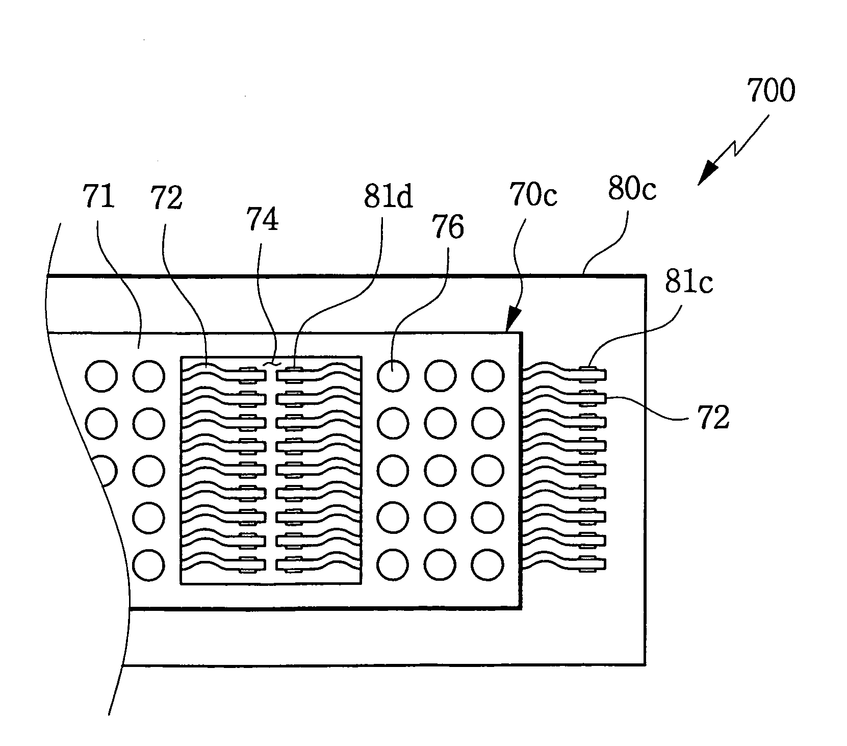
[0059]The chip pads of the IC chip can be arranged along peripheral regions and central regions of the top surface of the IC chip according to the present invention. As shown in FIG. 11, some chip pads 81c are arranged along peripheral regions and the other chip pads 81d are arranged along central regions.

[0060]To expose the chip pads 81c and 81d, a tape circuit substrate 70c not only has a smaller size than that of the IC chip 80c, but it also has an opening 74 at its central portion. The tape circuit substrate 70c has a base film 71 and beam leads 72, and an adhesive material (not shown) is interposed between the IC chip 80c and the tape circuit substrate 70c. The beam leads 72 formed on the bottom surface of the base film 71 are bonded to the chip pads 81c and 81d though the ILB process. Like the former embodiments, each beam lead 72 has a wavy portion capable of dispersing the stress produced during the ILB process. A sealing resin (not shown) encapsulates the opening 74 and the...


PUM


Abstract

A semiconductor chip package includes an IC chip and a tape circuit substrate. The tape circuit substrate has a base film and a plurality of beam leads formed on the base film. One end portion of each beam lead extends from the base film, and the extended portion has a widthwise wavy portion. The widthwise wavy portion may be, for example, semicircular shaped, S-shaped or zig-zag shaped. The IC chip has chip pads formed on a top surface thereof.

Description

[0001]This application claims priority from Korean Patent Application No. 2002-15179, filed on Mar. 11, 2003, the contents of which are incorporated herein by reference in their entirety.BACKGROUND OF THE INVENTION[0002]1. Field of the Invention[0003]The present invention relates to semiconductor packaging technology, and more particularly, to a semiconductor chip package having a tape circuit substrate with beam leads.[0004]2. Description of the Related Art[0005]With the current trend of high integration in semiconductor devices, semiconductor packaging and interconnect technologies are becoming very important. Moreover, as market demand for mobile handsets and liquid crystal displays (LCDs) increases, there will be a growing demand to make the semiconductor chip packages smaller, thinner, lighter, and more multifunctional. To meet this trend, several types of semiconductor packages using a tape circuit substrate have been developed and introduced. For example, a tape carrier packa...

Claims


Application Information

Patent Timeline
Patent Type & Authority Patents(United States)
IPC IPC(8): H01L23/48H01L21/60H01L23/495
CPCH01L23/49544H01L23/49551H01L23/49572H01L24/16H01L24/50H01L2224/13099H01L2924/01004H01L2924/01029H01L2924/01074H01L2924/01079H01L2924/01082H01L2924/12044H01L2924/14H01L2924/01006H01L2924/01033H01L2924/014H01L24/05H01L2224/05001H01L2224/05008H01L2224/05023H01L2224/05568H01L2224/05571H01L2924/00014H01L2224/05644H01L2224/05655H01L2224/05099H01L23/48
Inventor SON, DAE-WOOLEE, JIN-HYUKLEE, KWAN-JAI
Owner SAMSUNG ELECTRONICS CO LTD
Why Eureka
Try Eureka