Semiconductor device and method for manufacturing semiconductor device

a semiconductor and semiconductor technology, applied in semiconductor devices, semiconductor/solid-state device details, electrical devices, etc., can solve the problems of low mechanical strength, interlayer cracking, and low so as to reduce the mechanical strength of the insulating film, improve the reliability of interconnection, and suppress the adhesiveness between the insulating film and the upper and lower layers.

Inactive Publication Date: 2009-10-13
SONY CORP
View PDF7 Cites 2 Cited by
  • Summary
  • Abstract
  • Description
  • Claims
  • Application Information

AI Technical Summary

Benefits of technology

[0011]In such a semiconductor device, because the porosified insulating film includes the non-porous region, the density of the insulating film is enhanced and the contact areas with the upper and lower layers are increased corresponding to the existence of the non-porous region compared with a semiconductor device that includes an insulating film of which entire region is porosified. This suppresses the lowering of the mechanical strength of the insulating film and the lowering of the adhesiveness with the upper and lower layers.
[0014]As described above, in the semiconductor device and the manufacturing method thereof according to the embodiments of the present invention, the lowering of the mechanical strength of an insulating film and the lowering of the adhesiveness between the insulating film and the upper and lower layers are suppressed. Thus, the interconnect reliability can be improved, which can enhance the quality and performance of the semiconductor device.

Problems solved by technology

However, when a porosified interlayer insulating film is used, although the capacitance between interconnects is decreased, there are problems that the mechanical strength is significantly low and typically the adhesiveness with the lower and upper layers is also low.
Accordingly, the following troubles easily occur regarding formation of Cu buried interconnects by a dual damascene method: separation between the porosified interlayer insulating film and the upper and lower layers in a step for removing unnecessary interconnect patterns by chemical mechanical polishing (CMP); dicing crack in a packaging step; and interlayer crack in a bonding step.

Method used


Image

  • Semiconductor device and method for manufacturing semiconductor device
  • Semiconductor device and method for manufacturing semiconductor device
  • Semiconductor device and method for manufacturing semiconductor device

Examples


modification example

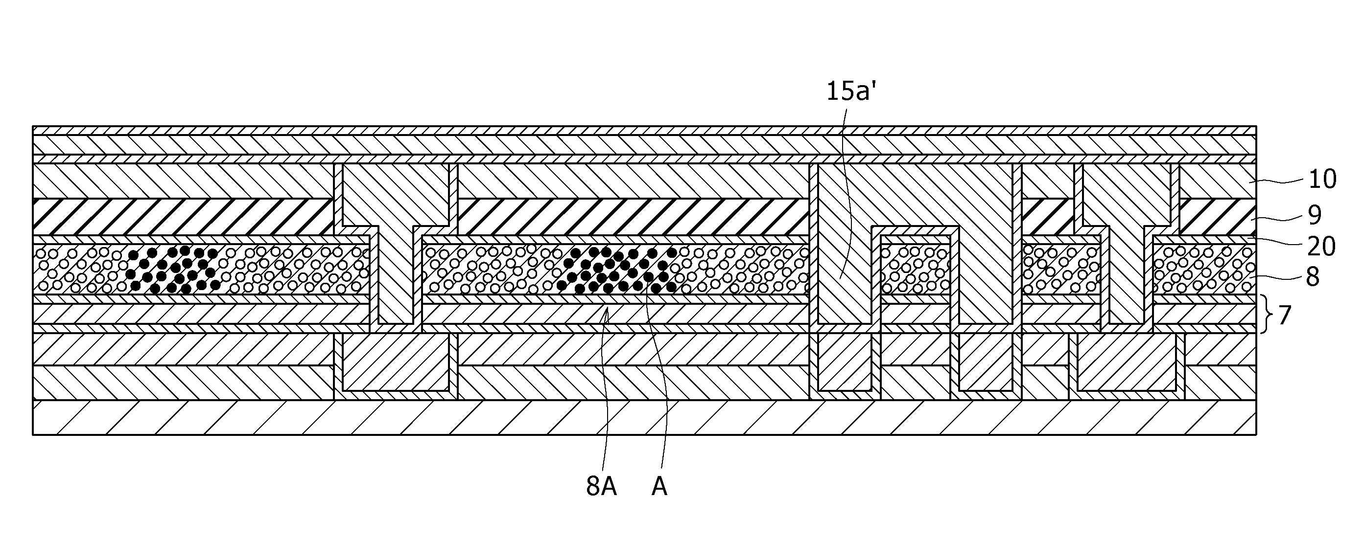
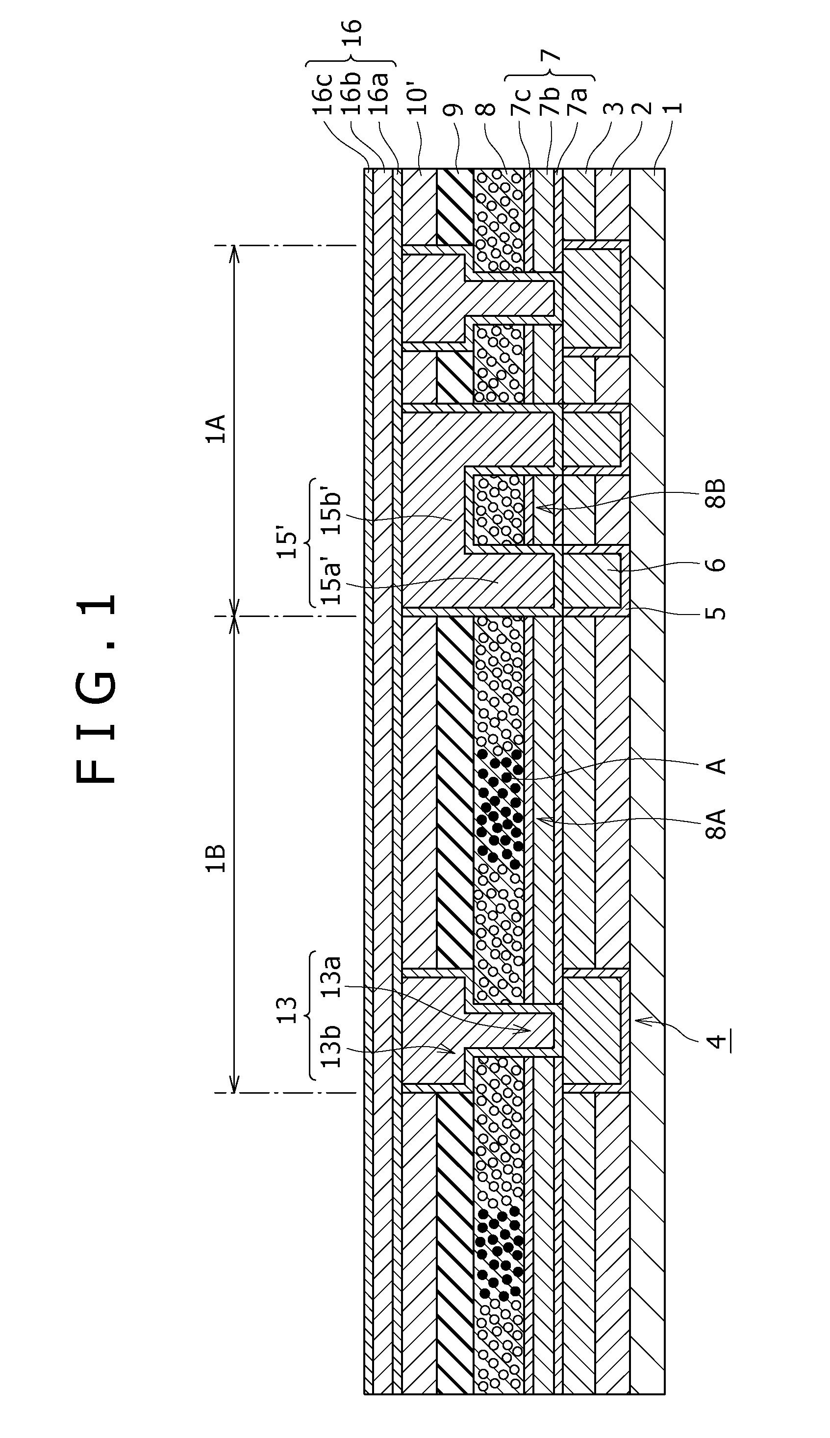
[0058]In the above-described embodiment example, the second insulating film 9 serves as a covering insulating film. However, as shown in FIG. 4, a covering insulating film 20 may be provided between the first insulating film 8 and the second insulating film 9. It is preferable that the covering insulating film 20 be a non-porous low dielectric constant material film, and it has a film thickness of 5 nm to 15 nm. In this example, the covering insulating film 20 composed of SiOC and having a film thickness of 15 nm is provided. When the covering insulating film 20 is thus interposed, the covering insulating film 20 prevents the porogen A from being removed through its decomposition from the upper side of the first insulating film 8, and therefore it is preferable that the second insulating film 9 be formed of a SiOC or PAE porous insulating film.

[0059]In this case, the vias 15a′ are provided in the covering insulating film 20, the first insulating film 8, and the etching stopper film ...


PUM


Abstract

Disclosed herein is a semiconductor device including: an insulating film configured to be provided on a substrate and be porosified through decomposition and removal of a pore-forming material; a covering insulating film configured to be provided on the insulating film; and conductive layer patterns configured to be provided in the covering insulating film and the insulating film and reach the substrate, wherein the insulating film includes a non-porous region in which the pore-forming material remains.

Description

CROSS REFERENCES TO RELATED APPLICATIONS[0001]The present invention contains subject matter related to Japanese Patent Application JP 2006-238628 filed in the Japan Patent Office on Sep. 4, 2006, the entire contents of which being incorporated herein by reference.BACKGROUND OF THE INVENTION[0002]1. Field of the Invention[0003]The present invention relates to a semiconductor device and a method for manufacturing a semiconductor device, and more particularly to a semiconductor device that includes a porosified insulating film and has a multilevel interconnect structure based on a damascene structure and a method for manufacturing the same.[0004]2. Description of the Related Art[0005]In step with miniaturization and increase in the integration degree of semiconductor devices, delay of electrical signals attributed to the time constant of interconnects is increasingly becoming a serious problem. To address this, for conductive layers in a multilevel interconnect structure, use of copper...

Claims


Application Information

Patent Timeline
Patent Type & Authority Patents(United States)
IPC IPC(8): H01L23/48H01L21/28
CPCH01L21/76811H01L21/7682H01L21/76832H01L23/53295H01L23/53238H01L23/5329H01L21/76835H01L2924/0002H01L2221/1047H01L2924/00H01L21/28
Inventor KAGAWA, YOSHIHISASHIMAYAMA, TSUTOMUKAMESHIMA, TAKATOSHI
Owner SONY CORP
Why Eureka
Try Eureka