Multi-layer wiring board, method for producing multi-layer wiring board, polishing machine for multi-layer wiring board, and metal sheet for producing wiring board

a multi-layer wiring and metal plate technology, applied in the direction of manufacturing tools, printing element electric connection formation, lapping machines, etc., can solve the problems of high integration difficulty, high cost, and difficulty in reducing the size of the above upper and lower wiring interconnecting hole, so as to reduce the number of wiring film forming steps, the effect of reducing the cost of multi-layer wiring board and low mechanical strength

Inactive Publication Date: 2005-05-12
INVENSAS CORP
View PDF7 Cites 53 Cited by
  • Summary
  • Abstract
  • Description
  • Claims
  • Application Information

AI Technical Summary

Benefits of technology

[0018] According to further another manufacturing method of the present invention, a plural kinds of basic wiring boards with a multi-layer wiring structure are prepared and a plurality of basic wiring boards including different kinds of boards from among the plural kinds of basic wiring boards are laminated. As a result, a multi-layer wiring board with multi-layers, for example, 4 layers to 10 or more layers can be easily obtained.
[0019] According to further another manufacturing method of the present invention, after the plurality of basic wiring boards are laminated, wiring film forming metal layers as the uppermost layer and the lowermost layer are patterned. Thus, wiring films on the uppermost layer and the lowermost layer can be simultaneously formed, so that the number of wiring film forming steps can be reduced by one, and the cost of the multi-layer wiring board can be reduced.
[0020] According to further another manufacturing method of the present invention, a multi-layer metal plate, each layer of which is thin and its mechanical strength is low, is reinforced with a reinforcing layer. Thus, workability is improved and a fraction defective can be reduced. In addition, the surface of a wiring film forming metal layer is continuously protected by the reinforcing layer during a period from the first step to the wiring film patterning step. Thus, damage or the like to the surface in for example a press step is prevented and a defect is not caused in a formed wiring film. Further, the surface of the wiring film forming metal layer is protected from a chemical solution and deposition of contaminants on the surface is prevented.
[0021] According to further another manufacturing method of the present invention, the same effect as the multi-layer wiring board manufacturing method in the preceding paragraph or the paragraph prior to the preceding paragraph can be obtained. In addition, when a reinforcing layer is made of metal such as nickel or copper, etching is required for peeling it so that the number of steps is increased. However, in the case where the reinforcing layer is composed of a peeling layer and a heat resistant film as in this multi-layer wiring board manufacturing method, when a wiring film patterning step is to be conducted, it is sufficient that the heat resistant film is merely peeled off so that the process is simplified as a result.
[0022] According to a wiring board forming metal plate of the present invention, a multi-layer metal plate, each layer of which is thin and its mechanical strength is low, is reinforced with a reinforcing layer. Thus, workability is improved and a fraction defective can be reduced. In addition, the surface of a wiring film forming metal layer is continuously protected by a heat resistant film during a period of from the first step to the wiring film patterning step. Thus, damage or the like to the surface in, for example, a press step is prevented and a defect is not caused in a formed wiring film. Further, the surface of the wiring film forming metal layer is protected from a chemical solution and deposition of contaminants on the surface is prevented. Furthermore, when the reinforcing layer is made of metal such as nickel or copper, etching is required for peeling it so that the number of steps is increased. However, in the case where the metal plate for wiring board formation is composed of a peeling layer and a heat resistant film, when a wiring film patterning step is to be conducted, it is sufficient that the heat resistant film is merely peeled off so that the process is simplified as a result.

Problems solved by technology

By the way, according to the above conventional high-density multi-layer wiring board manufacturing method, there is a problem that high integration is difficult to achieve.
This is because it is difficult to reduce a size of the above upper and lower wirings interconnecting hole.
When mass production and a yield are considered, it is difficult in practice to set the hole size to 0.3 mm or less in the core board and high integration is limited by the existence of the upper and lower wirings interconnecting hole having a relatively large hole size.
Thus, when the hole size is large, this is a factor for directly limiting the integration of the wiring board.
Therefore, when the hole size is increased, this becomes a factor for increasing the number of wiring films that are forced to make a detour and also increasing the detour length of the detouring wiring film, and indirectly limits the integration of the wiring board.
However, with only pressure welding, electrical connection is not provided from the beginning, or even if the electrical connection is provided, by an accelerating test in which long-term usage is assumed, there is observed a phenomenon such that a pressure welding surface is deteriorated, or in some extreme cases, the electrical connection is lost.
Specifically, copper oxide or other such coating film progresses due to a phenomenon in which a resin composing an insulating layer and other foreign matters such as, moisture, hydrogen, and the like gradually penetrate into the pressure welding portion, or the progress of oxidation on a pressure welding surface between the bump and the copper layer or the wiring film, so that a problem is cased in that an electrical resistance value between the bump and the copper layer or the wiring film is increased, thus reducing the long-term connection reliability.

Method used


Image

  • Multi-layer wiring board, method for producing multi-layer wiring board, polishing machine for multi-layer wiring board, and metal sheet for producing wiring board
  • Multi-layer wiring board, method for producing multi-layer wiring board, polishing machine for multi-layer wiring board, and metal sheet for producing wiring board
  • Multi-layer wiring board, method for producing multi-layer wiring board, polishing machine for multi-layer wiring board, and metal sheet for producing wiring board

Examples


first embodiment

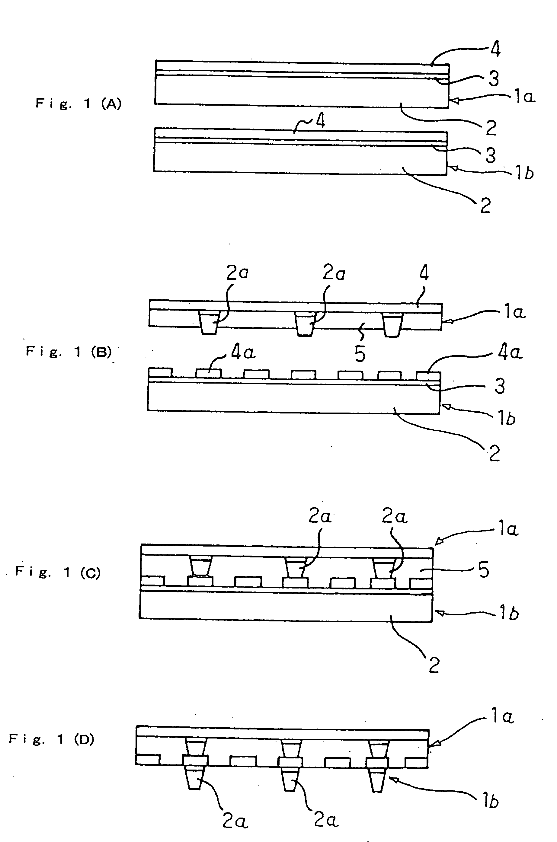
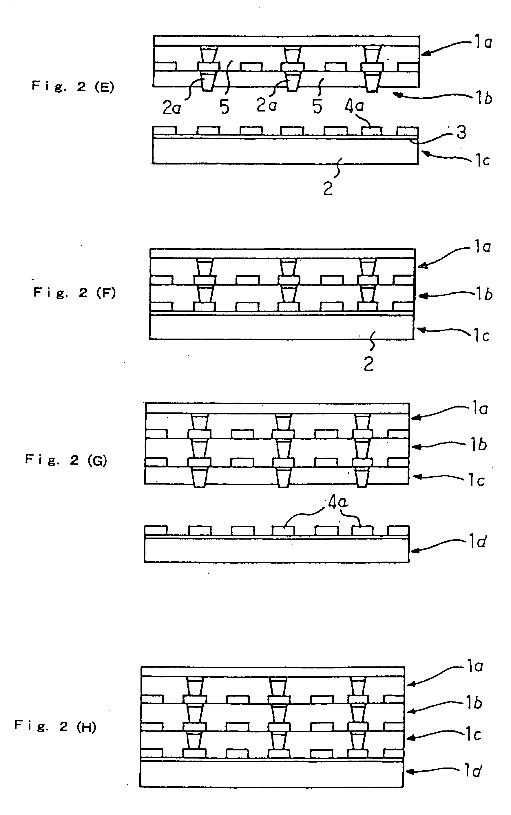
[0066] FIGS. 1(A) to 1(D), FIGS. 2(E) to 2(H), and FIGS. 3(I) to 3(K) are sectional views showing steps of FIGS. 1(A) to 3(K) in order in a first embodiment mode of a multi-layer wiring board manufacturing method according to the present invention.

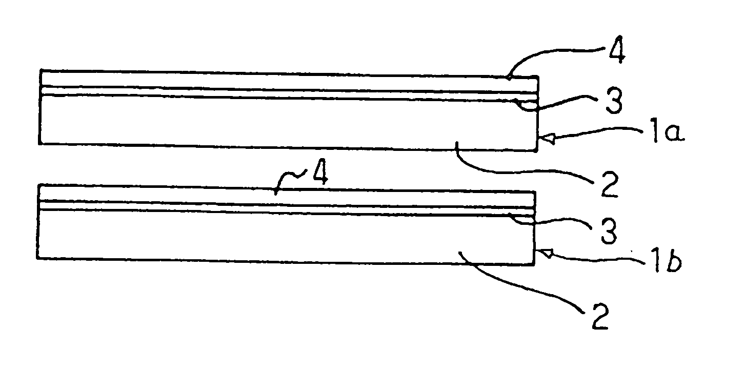
[0067] (A) First, as shown in FIG. 1(A), multi-layer metal plates 1a and 1b are prepared. Note that the multi-layer metal plate 1a corresponds to a first multi-layer metal plate in claim 1 and the multi-layer metal plate 1b corresponds to a second multi-layer metal plate of claim 1.

[0068] The above multi-layer metal plates 1a and 1b each are obtained by laminating a wiring film forming metal layer 4 made of copper foil having a thickness of for example 18 μm on one main surface of a bump forming metal layer 2 made of copper foil having a thickness of for example 100 μm, through an etching stop layer 3 made of a nickel layer having a thickness of for example 2 μm.

[0069] (B) Next, with respect to the above multi-layer metal plate 1a, the b...

second embodiment

[0091] FIGS. 4 to 11 are explanatory views of a second embodiment mode of a multi-layer wiring board manufacturing method according to the present invention. According to this embodiment mode, a row material is processed to prepare plural types of basic wiring boards 50 (for example, 50α, 50β, 50γ and 50δ) composing a multi-layer wiring board, and arbitrary boards are combined from the plural types of basic wiring boards and laminated to produce a multi-layer wiring board 51 (for example, 51a, 51b, 51c or 51d). FIGS. 4 to 7 are explanatory views of a basic wiring board manufacturing method or respective basic wiring boards. FIGS. 4(A) to 4(D) show a method of manufacturing a first example 50α of the basic wiring boards in step order. FIG. 5 shows a second example 50β of the basic wiring boards. FIG. 6 shows a third example 50γ of the basic wiring boards. FIG. 7 shows a fourth example 50δ of the basic wiring boards.

[0092] First, a method of manufacturing the first example 50α will be...

third embodiment

[0108] FIGS. 12(A) to 12(E), and FIGS. 13(F) to 13(I) are sectional views showing in order steps (A) to (I) in accordance with a third embodiment mode of a multi-layer wiring board manufacturing method of the present invention.

[0109] (A) A multi-layer metal plate 20a in which a wiring film forming metal layer 23 (not shown) made of copper foil is laminated on one of surfaces of a bump forming metal layer 21 made of copper foil through an etching stop layer 22 made of nickel is prepared, and the wiring film forming metal layer 23 is patterned by selective etching to form wiring films 23a. At this time, the etching stop layer 22 acts to prevent the bump forming metal layer 21 from being etched. FIG. 12(A) shows a state after the formation of the wiring films 23a.

[0110] (B) Next, as shown in FIG. 12(B), a thin copper film 24 is plated on a wiring film 23a forming side surface of the multi-layer metal plate 20a. The copper film 24 acts to prevent etching of an etching stop layer (25), ...


PUM

PropertyMeasurementUnit
hole sizeaaaaaaaaaa
thicknessaaaaaaaaaa
thicknessaaaaaaaaaa

Abstract

A plurality of multi-layer metal plates (1) each being composed of a bump forming metal layer (2), an etching stop layer (3), and a wiring film forming metal layer (4), and in which a wiring film (4a) is formed from the wiring film forming metal layer and a bump 2a is formed from the bump forming metal layer are prepared, and on a bump forming surface of a multi-layer metal plate, a wiring film of another multi-layer metal plate is overlapped. Such lamination process is repeated in succession for multi-layering. In addition, a polishing machine for multi-layer wiring board (11a) which includes metal plate holding means (13) for holding a metal plate (1a), cutter holding means (25) for holding a cutter (26) above the metal plate, height adjustment mechanism (20) for adjusting the height of the cutter holding means, and cutter parallel moving mechanism (15) for relatively moving the cutter holding means in parallel to the surface of the metal plate is used to conduct polishing.

Description

TECHNICAL FIELD [0001] The present invention relates to a method of manufacturing a multi-layer wiring board and a metal plate for forming the multi-layer wiring board, and more particularly to a multi-layer wiring board manufacturing method of manufacturing a high integration, high reliability wiring board having a microvia to a metal plate for forming a high integration, high reliability wiring board having a microvia. BACKGROUND ART [0002] When high integration is to be obtained for a wiring board, it is required that the wiring board is multi-layered and connections between upper and lower wiring films are minutely formed with high reliability. The present invention responds to such requirement. [0003] By the way, conventionally, there is a technique in which with respect to a multi-layer wiring board, for example, a wiring board in which wiring films are formed on both surfaces or in a multi-layer structure is used as a base (hereinafter referred to as “a core board” in some ca...

Claims


Application Information

Patent Timeline
Patent Type & Authority Applications(United States)
IPC IPC(8): B24B1/00B24B7/22B24B37/04H05K3/06H05K3/40H05K3/46
CPCB24B1/00B24B7/228B24B37/04H05K3/06H05K3/4038H05K3/4614Y10T29/5313H05K2201/0355H05K2203/0143H05K2203/025H05K2203/0384H05K2203/061H05K3/4652
Inventor IIJIMA, TOMOOKATO, YOSHIROODAIRA, HIROSHIOHSAWA, MASAYUKIKUROSAWA, INETAROSAKUMA, KAZUOASANO, TOSHIHIKOENDO, KIMITAKA
Owner INVENSAS CORP
Why Eureka
Try Eureka