

Solder material and electric or electronic device in which the same is used
a technology of electric or electronic devices and solder materials, which is applied in the direction of soldering apparatus, welding/cutting media/materials, manufacturing tools, etc., can solve the problems of low melting point of solder material, poor mechanical strength of alloy material having brittleness, and poor mechanical strength
- Summary
- Abstract
- Description
- Claims
- Application Information
AI Technical Summary
Benefits of technology
Problems solved by technology
Method used
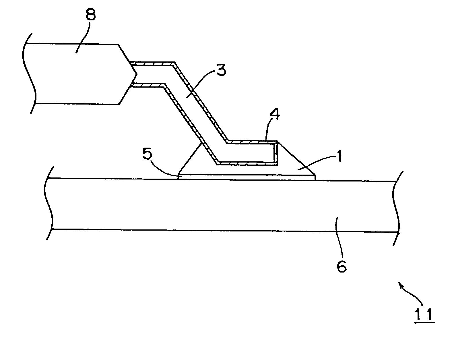
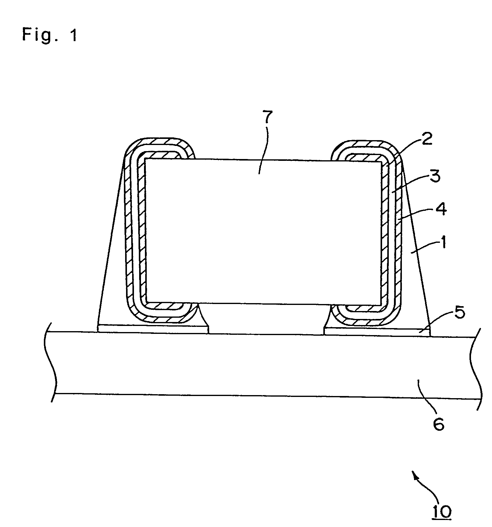
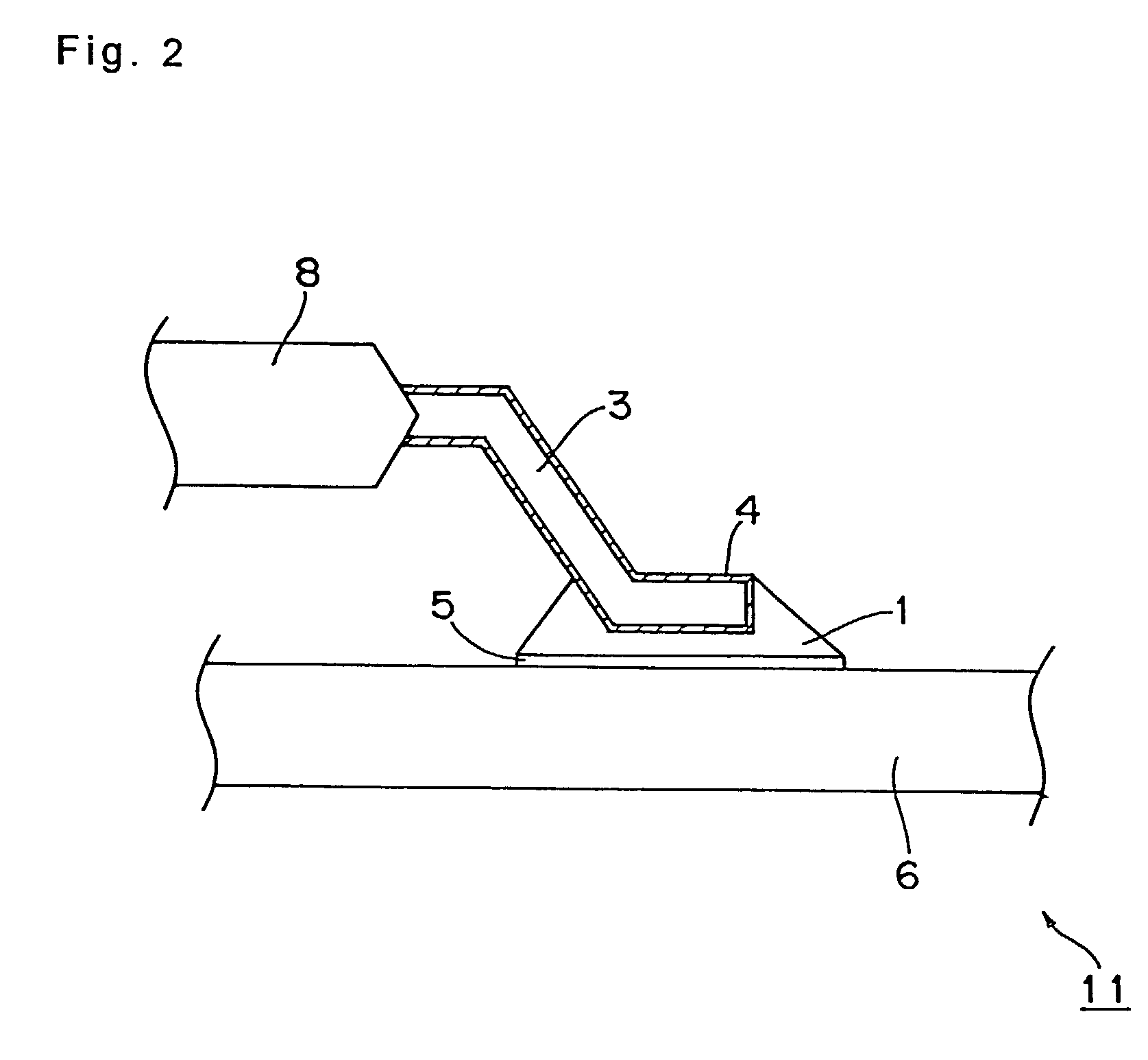
Image

Examples
example 1
[0055] In this example, a solder material was prepared by melting and blending metal materials at a composition ratio as shown in Tables 5 to 16, so that various solder materials were produced. It is to be noted that a ratio of Sn is not shown in Tables 5 to 16, but the ratio of Sn corresponds to the balance which is resulted by deducting ratios of metal materials (or elements) shown in the Tables except Sn from 100. Further, each composition ratio is shown in a unit of "% by weight" on the basis of the whole as described above, and a blank in the Table shows not containing (i.e. a content of zero).
[0056] A melting point (m.p.) (.degree. C.) of each of thus prepared solder material was measured as a temperature at which the solder material completely melts by means of a differential thermal analyzer. The measured melting points are also shown in Tables 5 to 16.
[0057] Additionally, a tensile strength of each of the solder materials was measured by means of Instron tensile testing mac...
PUM
| Property | Measurement | Unit |
|---|---|---|
| melting point | aaaaa | aaaaa |
| melting point | aaaaa | aaaaa |
| melting point | aaaaa | aaaaa |
Abstract
Description
Claims
Application Information