Pattern matching method, image processing device, and computer program

a pattern matching and image processing technology, applied in image enhancement, instruments, using wave/particle radiation means, etc., can solve the problems of large deviation of image and inability to obtain appropriate matching positions, and achieve the effect of performing highly accurate regardless of deformation

Active Publication Date: 2015-09-22
HITACHI HIGH-TECH CORP
View PDF16 Cites 1 Cited by
  • Summary
  • Abstract
  • Description
  • Claims
  • Application Information

AI Technical Summary

Benefits of technology

[0010]According to the above-described configuration, pattern matching can be performed highly accurately regardless of deformation of an edge, variability of contrast, etc.

Problems solved by technology

Rough position alignment of a measurement position is performed by movement of a stage on which a wafer is mounted, however, in positioning accuracy of a stage, large deviation occurs on an image that is captured with high magnification by an electron microscope.
However, there is a case in which an appropriate matching position is not obtained because matching is not performed appropriately due to unexpected reflection of a lower layer pattern.

Method used


Image

  • Pattern matching method, image processing device, and computer program
  • Pattern matching method, image processing device, and computer program
  • Pattern matching method, image processing device, and computer program

Examples


first embodiment

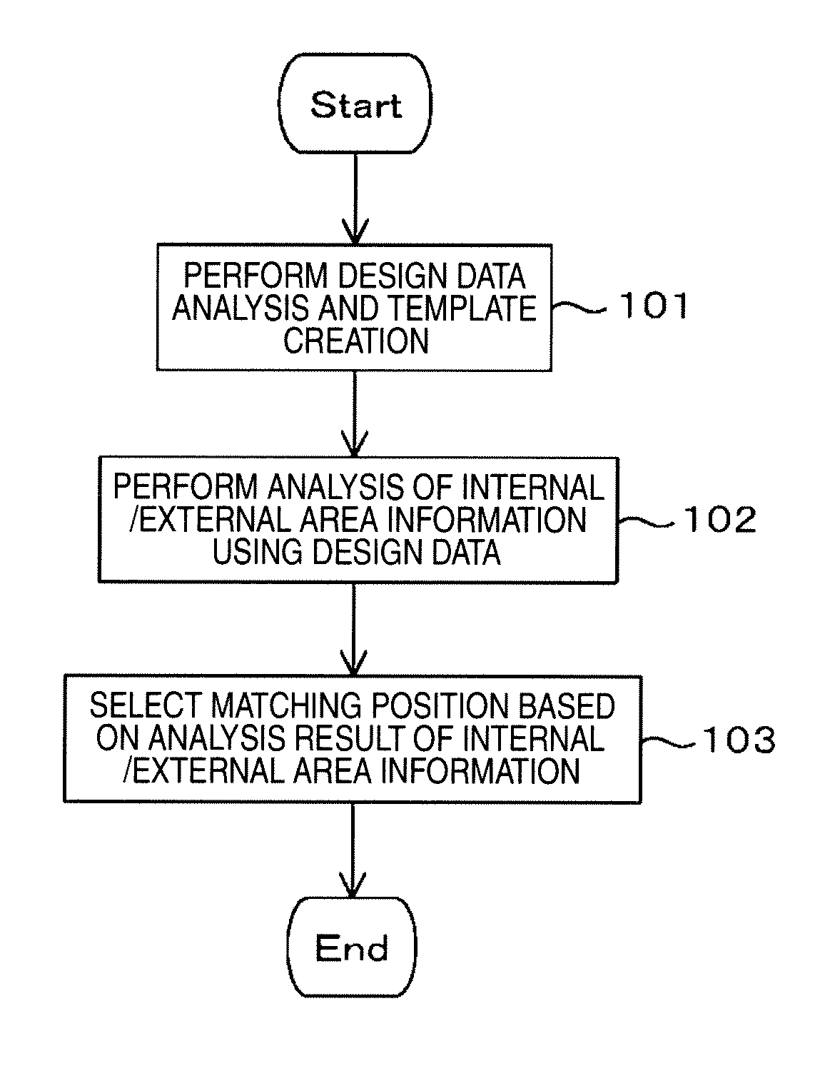
[0053]A pattern matching method according to a first embodiment can be applied to a system that performs measurement or examination of a semiconductor device. For example, in a measurement or examination process of a semiconductor device, measurement of dimensions, examination of a defect, etc. of design data and a pattern that is formed on a semiconductor device is performed. In the first embodiment, an example is described in which a template is created that is applied to pattern matching for identifying a measurement or examination position is created using design data that includes a portion on which measurement or examination is performed. It is noted that, an example is described below in which a desired pattern is searched for from an image captured by a scanning electron microscope (hereinafter, referred to as an SEM), however, the embodiment are not limited to the example. For example, the embodiment can also be applied to a case in which a desired pattern is searched for f...

second embodiment

[0108]In addition, the above-described characteristic quantity determination method of an area of interest can be used as a determination method of matching error. FIG. 16 is a flowchart illustrating an example of the determination method of matching error, and after executing the step 102 that is illustrated in FIG. 1, a step of comparing an analysis result with a threshold value (step 1601) or a step of comparing two or more analysis results (step 1602), and a step of determining matching failure on the basis of the comparison result (step 1603) are executed.

[0109]The steps 1601, 1602, and 1603 are described in detail. The analysis result that is obtained in the step 102 is given by a statistical quantity, and here, the analysis result is regarded as a standard deviation S. When matching is successfully performed, an ideal value of the standard deviation S is zero. In the step 1601, a standard deviation S and an optionally given threshold value are compared. Here, when the standar...

third embodiment

[0111]In addition, as the pattern matching method, pattern matching using only an area of interest can be performed. FIG. 17 is a flowchart illustrating an example of a matching method selectively using an area of interest, and after executing step 101 that is illustrated in FIG. 1, a step of performing matching using an optional image area that corresponds to the area of interest and an area on a template that corresponds to the area of interest (step 1701), and a step of selecting an optimal matching position on the basis of the matching result (step 1702) are executed.

[0112]Steps 1701 and 1702 are described in detail. FIG. 18 is a diagram illustrating a specific example of a matching method using a template that selectively uses an area of interest. Here, it is assumed that an SEM image and design data has a multi-layer structure, and the area of interest is in the external area of an upper layer. In step 1701, matching is performed using a lower layer template 1801 in which an a...


PUM


Abstract

In order to provide a computer program, an image processing device, and a pattern matching method that perform pattern matching at a high level of accuracy without relying on edge deformation, contrast fluctuations, etc., in one embodiment, the disclosed pattern matching method and device perform pattern matching over an image using a template produced on the basis of the below mentioned design data. The pattern matching method and device determine the characteristic quantities of the image for an inner region and / or an outer region that are divided by a line that defines the contour of a pattern, and determine positions at which said characteristic quantities satisfy predetermined conditions to be matching positions, matching position candidates, or erroneous matching positions.

Description

TECHNICAL FIELD[0001]The present invention relates to an image processing device that processes an image signal obtained by a scanning electron microscope, etc., and particularly relates to a template matching method on an image, an image processing device that realizes the template matching method, and a computer program.BACKGROUND ART[0002]Conventionally, a technology in which a certain given shape (template) is searched for in a target image has been widely used as template matching.[0003]In measurement of a pattern on a semiconductor wafer using a scanning electron microscope, the template matching is performed in order to obtain a measurement position (see Patent Literature 1). Rough position alignment of a measurement position is performed by movement of a stage on which a wafer is mounted, however, in positioning accuracy of a stage, large deviation occurs on an image that is captured with high magnification by an electron microscope. In order to perform measurement in an acc...

Claims


Application Information

Patent Timeline
Patent Type & Authority Patents(United States)
IPC IPC(8): G06K9/00G06K9/74G06T7/00H01J37/28G01B15/00G06K9/62G06K9/32G06V10/88
CPCG06K9/6201G01B15/00G06K9/3241G06K9/6223G06K9/74G06T7/001G06T7/003H01J37/28G06T2207/10061G06T2207/20036G06T2207/30148H01J2237/221H01J2237/2817G06T7/337G06V10/255G06V10/88G06V10/763G06F18/23213G06F18/22
Inventor USHIBA, HIROYUKITOYODA, YASUTAKAABE, YUICHIIKEDA, MITSUJI
Owner HITACHI HIGH-TECH CORP
Why Eureka
Try Eureka