
Multi-channel transceiver

a transceiver and multi-channel technology, applied in the field of multi-channel transceivers, can solve the problems of reducing power, needing to dissipate heat, and general non-favorable use of such vcsels, and achieves the effects of reducing power consumption, small size, and fewer optical alignment steps

Inactive Publication Date: 2015-10-13
TE CONNECTIVITY NEDERLAND
View PDF20 Cites 8 Cited by
  • Summary
  • Abstract
  • Description
  • Claims
  • Application Information

AI Technical Summary

Benefits of technology

[0006]The present invention provides a transceiver having relatively few optical alignment steps, a relatively small size, and relatively lower power consumption. Specifically, the transceiver of the present invention uses direct modulated long-wavelength VCSELS, which offers a number of benefits. For example, the use of such VCSELs reduces the power and thus the need to dissipate heat. This is especially helpful in multi-channel transceivers having high density transmitters and drive circuitry. The electronics can work more efficiently and therefore less airco units are needed to cool the systems. Furthermore, because the VCSEL may be fabricated in arrays, they reduce fabrication cost per transceiver considerably. For example, by aligning bars of 12 components the number of alignment steps is reduced. The compact arrays also reduce the footprint of the transceiver substantially. Still more benefits will become obvious to those of skill in the art in light of this disclosure.

Problems solved by technology

For example, the use of such VCSELs reduces the power and thus the need to dissipate heat.
The use of such VCSELs is unobvious and is generally not favored for long-wavelength applications because VCSELs at such wavelengths do not lend themselves to flip chip mounting.
Although wire bonding is a well known and reliable technology, it is generally discouraged for high speed applications such as those generally encountered in optical communications.
Applicants have realized, however, that in fiber-to-the-home applications, high speed operation is not as important as the reliability and manufacturability of the transceivers.
Therefore, even though the VCSELs may need to be wire bonded to the substrate and thus may be limited in operating frequencies, such limitations are outweighed by the aforementioned benefits of the VCSEL array configurations that VCSELs afford.

Method used


Image

  • Multi-channel transceiver
  • Multi-channel transceiver
  • Multi-channel transceiver

Examples


Embodiment Construction

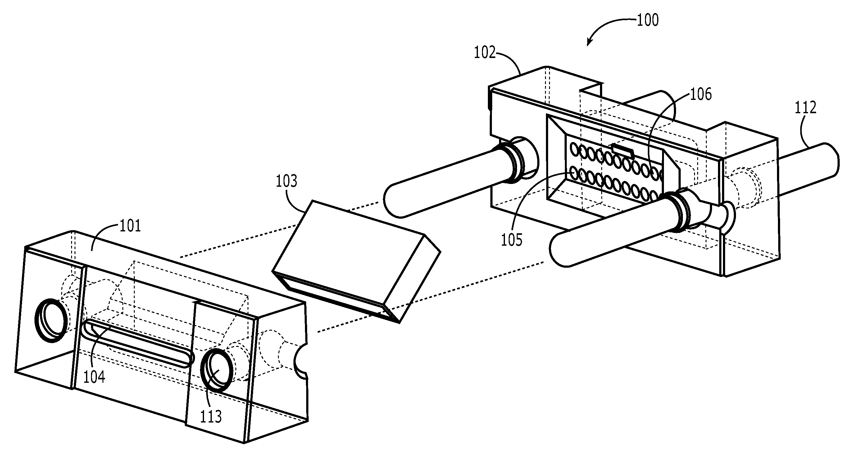
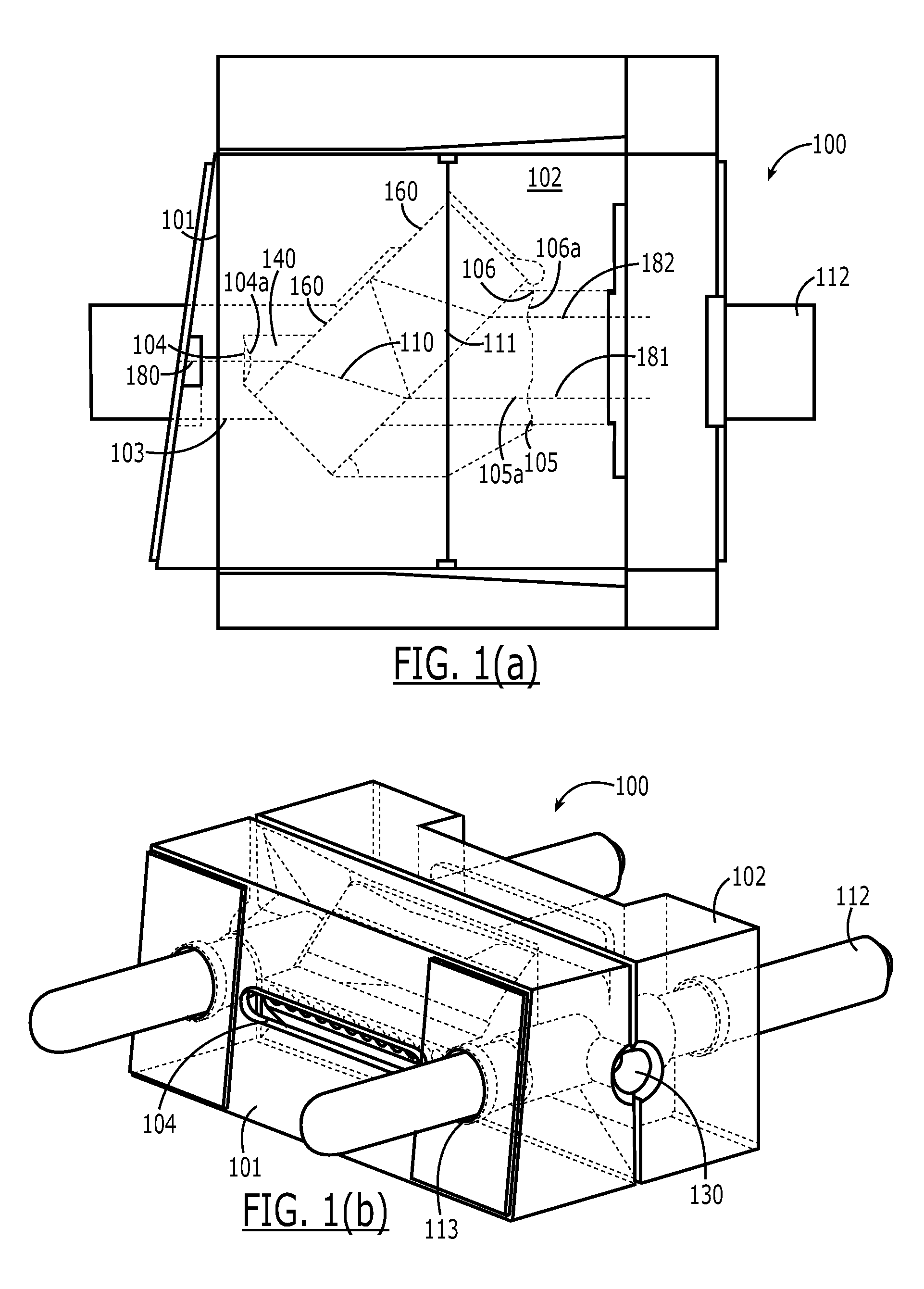
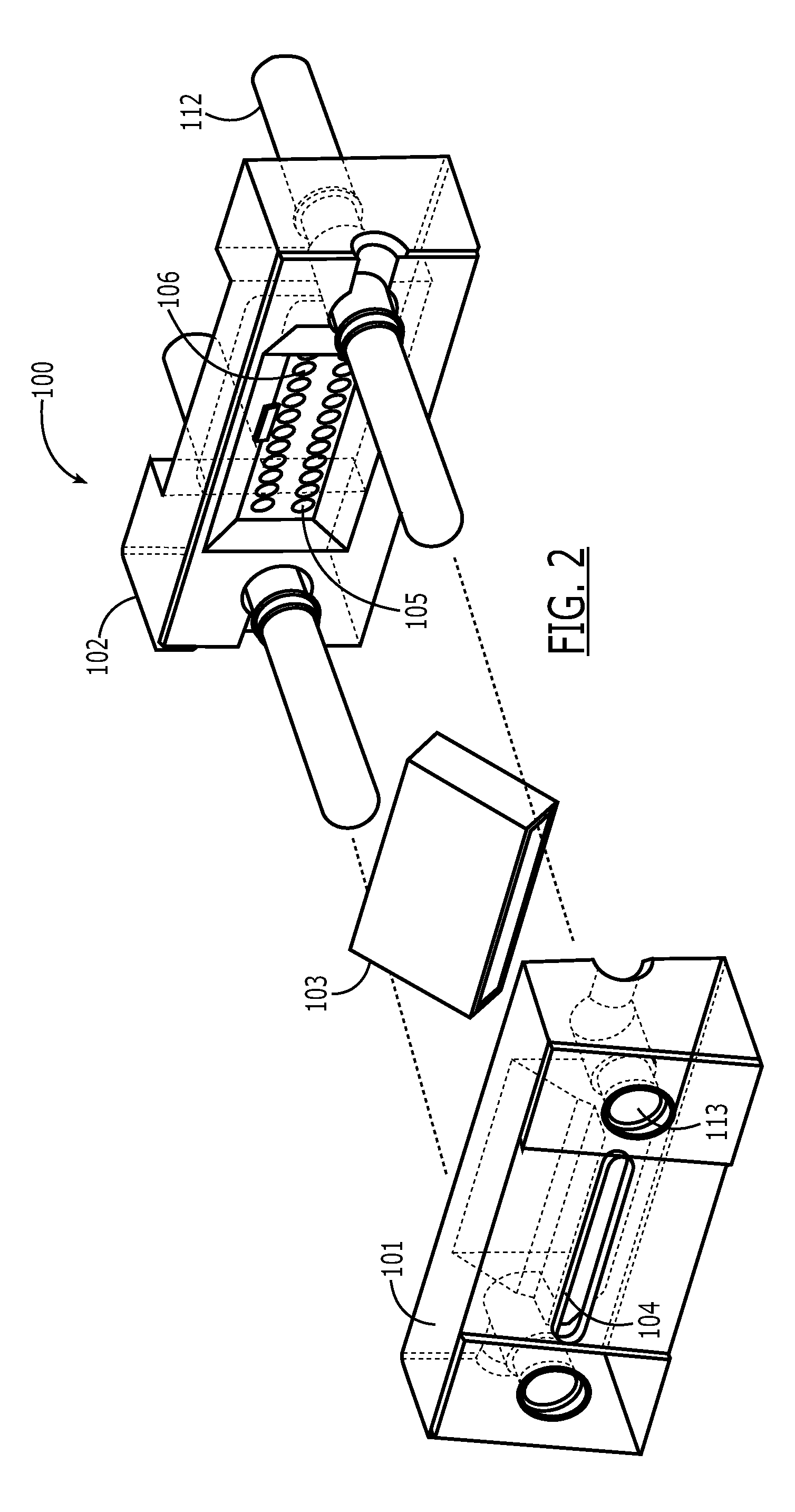
[0022]Referring to FIGS. 1(a), 1(b) and 2, one embodiment of the optical interface 100 of the present invention is shown. As used herein, an optical interface refers to the interface between an optical conductor and one or more optical devices, which are typically, although not necessarily, opto-electric devices (OEDs).

[0023]The optical interface 100 comprises a first portion 101 having at least one optical conduit interface 104 with a first axis 180 for optically coupling with at least one optical conduit (not shown). The optical interface 100 also comprises a second portion 102 having at least one transmitter interface 105 with a second axis 181 for optically coupling with a transmitting optical device (not shown), and at least one receiver interface 106 with a third axis 182 for optically coupling with a receiving optical device (not shown). The first, second and third axes are essentially parallel. Disposed between the first and second portions 101, 102 is a wavelength filter el...


PUM


Abstract

A transceiver comprising at least one chip comprising at least a first array of long-wavelength VCSELs and at least a second array of receiving optical devices, an optical interface optically coupled to the VCSELs and the receiving optical devices and configured to optically couple with an optical connector, transmitting and receiving circuitry electrically connected the VCSELs and the receiving optical devices, and adapted for connecting to an electrical connector, and a frame for holding the chip, the optical interface, and the transmitting and receiving circuitry.

Description

REFERENCE TO RELATED APPLICATION[0001]This application to U.S. Provisional Application No. 61 / 538,245 filed Sep. 23, 2011, the entire disclosure of which is hereby incorporated herein by reference. This application is also related to concurrently filed U.S. application Ser. No. 13 / 623,479 entitled “Optical Interface for Bidirectional Communications”, incorporated herein by reference.FIELD OF INVENTION[0002]The subject matter herein relates generally to transceivers, and more particularly, to a multi-channel transceiver configuration that facilitates manufacturability.BACKGROUND OF INVENTION[0003]Fiber optic components are used in a wide variety of applications. The use of optical fibers as a medium for transmission of digital data (including voice, interne and IP video data) is becoming increasingly more common due to the high reliability and large bandwidth available with optical transmission systems. Fundamental to these systems are transceivers for transmitting and receiving opti...

Claims


Application Information

Patent Timeline
Patent Type & Authority Patents(United States)
IPC IPC(8): G02B6/12G02B6/42H04B10/00H04B10/40
CPCH04B10/14G02B6/4246H04B10/40G02B6/4292G02B6/4249
Inventor DUIS, JEROEN ANTONIOUS MARIARIETVELD, JAN WILLEMVOS, JOSEPH GERARDUS MARIA
Owner TE CONNECTIVITY NEDERLAND
Learn More