Thermal detector, thermal detection device, and electronic instrument
a technology of thermal detection element and thermal isolation, which is applied in the direction of instruments, optical radiation measurement, and sensing radiation from moving bodies, can solve the problem of inability to reliably ensure the thermal isolation of the thermal detection element from the substrate, and achieve the effect of reliably providing the thermal isolation
- Summary
- Abstract
- Description
- Claims
- Application Information
AI Technical Summary
Benefits of technology
Problems solved by technology
Method used
Image
Examples
modification examples
7. Modification Examples
7.1. First Modification Example
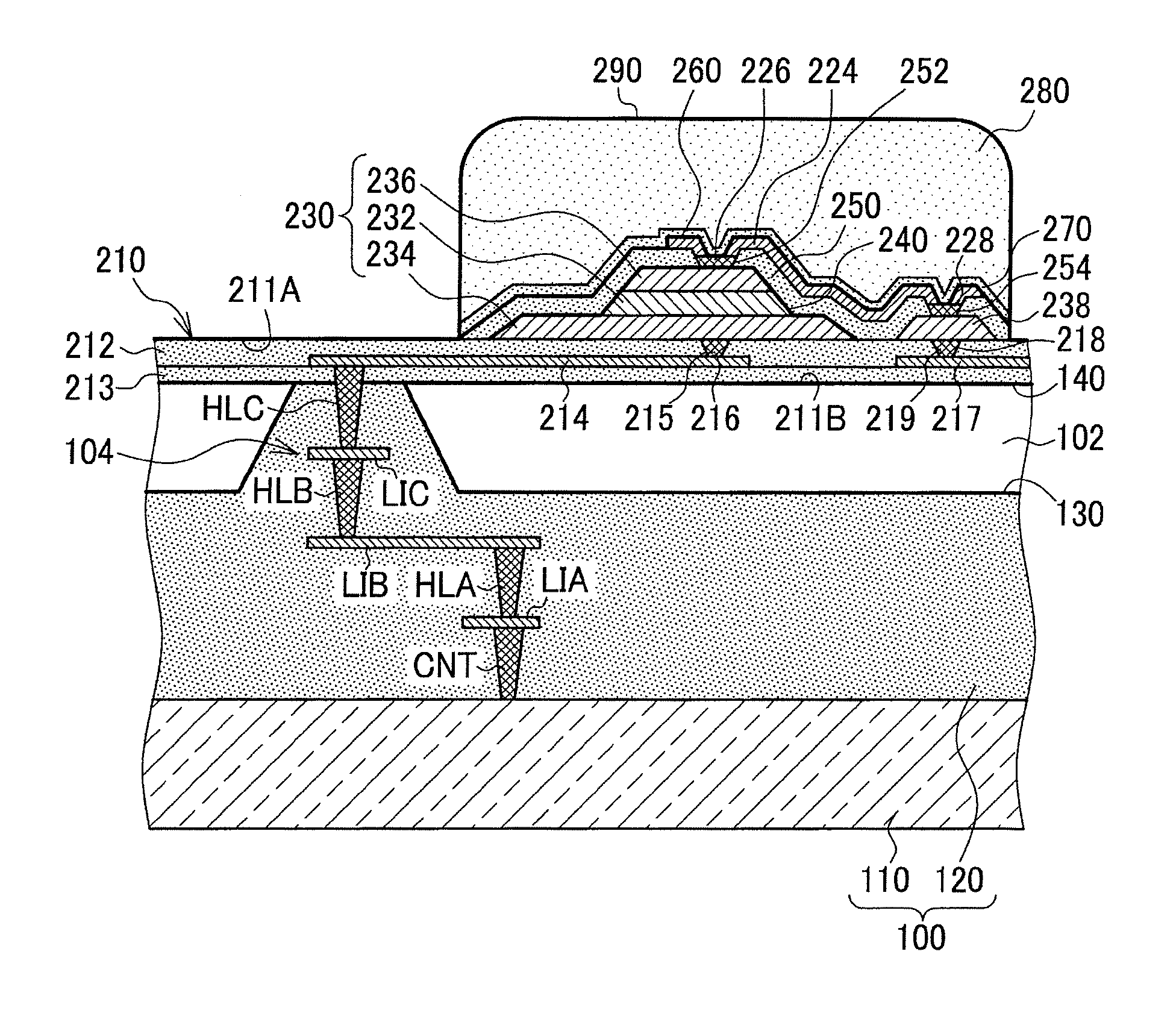
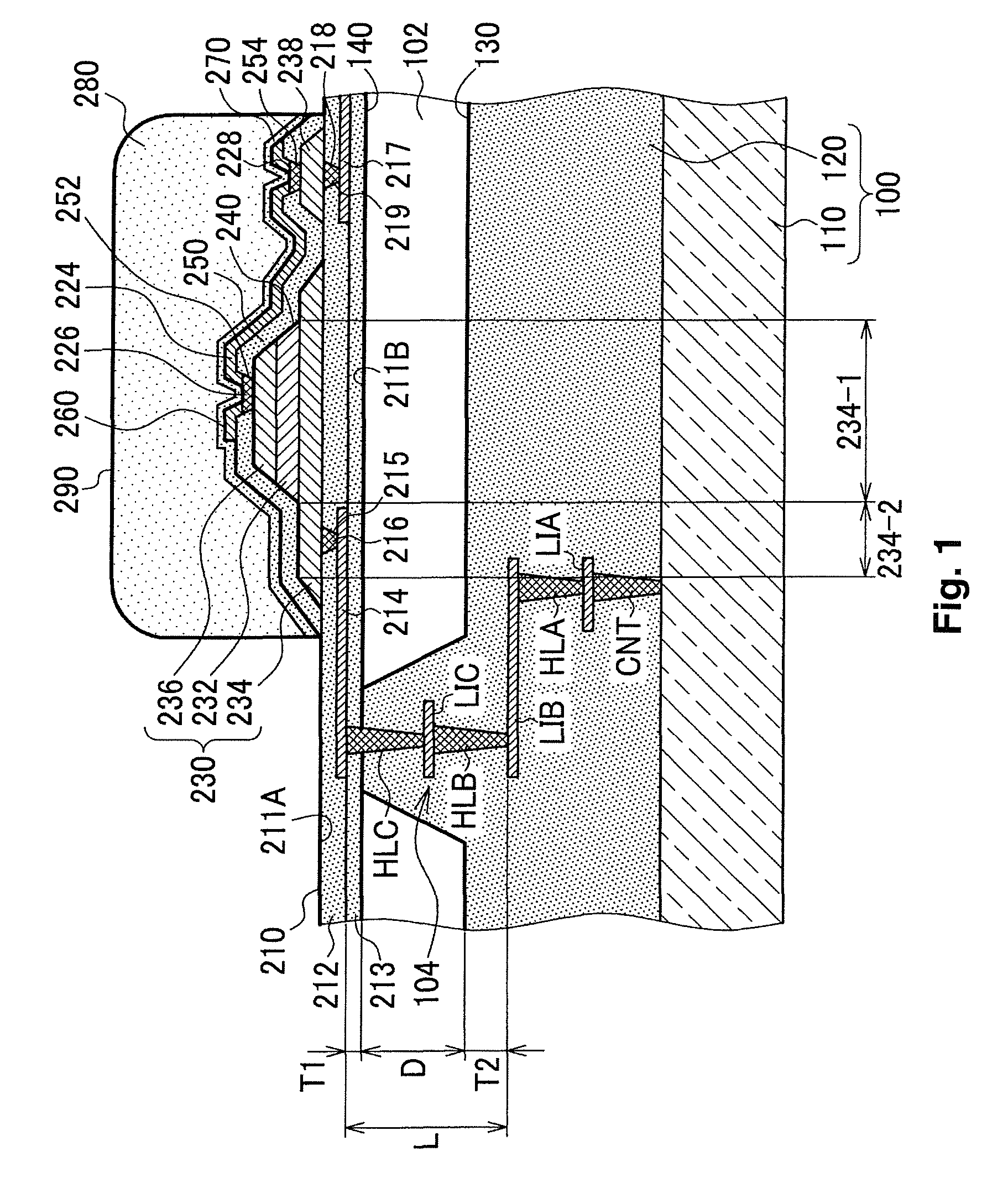
[0108]As shown in FIG. 5, the first hole 215 is at a position that faces the first electrode 234 and the first wiring layer 214 and may be formed through to the first layer member 212 at a position that is opposite the capacitor 230. The first plug 216 is embedded in the first hole 215 that is formed in a position that is opposite the capacitor 230.
[0109]In FIG. 5, a material such as tungsten (W) having high step coverage (step filmability) is preferably used for the first plug 216 The first surface 211A of the support member 210 affects the orientation of the capacitor 230, and thus planarity is desired.
[0110]In this embodiment as well, the wiring that connects to the first electrode 234 can be formed by the first wiring layer 214 and the first plug 216 formed on the support member 210. The first plug 216 is formed on the support member 210 at a position that is opposite the capacitor 230, and thus the element surface area is n...
second modification example
7.2. Second Modification Example
[0112]In FIG. 6, in contrast to FIGS. 1 and 5, the first and second wiring layers 214, 217 that respectively connect with the first and second electrodes 234, 236 are not provided on the support member 210. Rather, the first and second electrode wiring layers 222, 224 that connect respectively with the first and second electrodes 234, 236 are provided on the interlayer insulating layer 250.
[0113]An intermediary conductive layer 238 is formed on the first surface 211A in the substrate member 210 on the post 104 shown in FIG. 6. The interlayer insulating layer 250 is formed so that it covers the intermediary conductive layer 238. The second electrode wiring layer 222 is formed on the interlayer insulating layer 250. The second electrode wiring layer 222 is in continuity with the intermediary conductive layer 238. In the structure of FIG. 6, the step shape shown in FIG. 3 is formed in the arm part of the support member 210.
[0114]In addition, in FIG. 6, t...
PUM
 Abstract
Description
Claims
Application Information


