Organic light emitting diode display, manufacturing method thereof, and rotating device for circuit film

a technology of light-emitting diodes and manufacturing methods, applied in the direction of semiconductor devices, electrical devices, transistors, etc., can solve the problems of adhesion reliability deterioration, and achieve the effect of reducing the dead spa

Active Publication Date: 2015-11-17
SAMSUNG DISPLAY CO LTD
View PDF15 Cites 2 Cited by
  • Summary
  • Abstract
  • Description
  • Claims
  • Application Information

AI Technical Summary

Benefits of technology

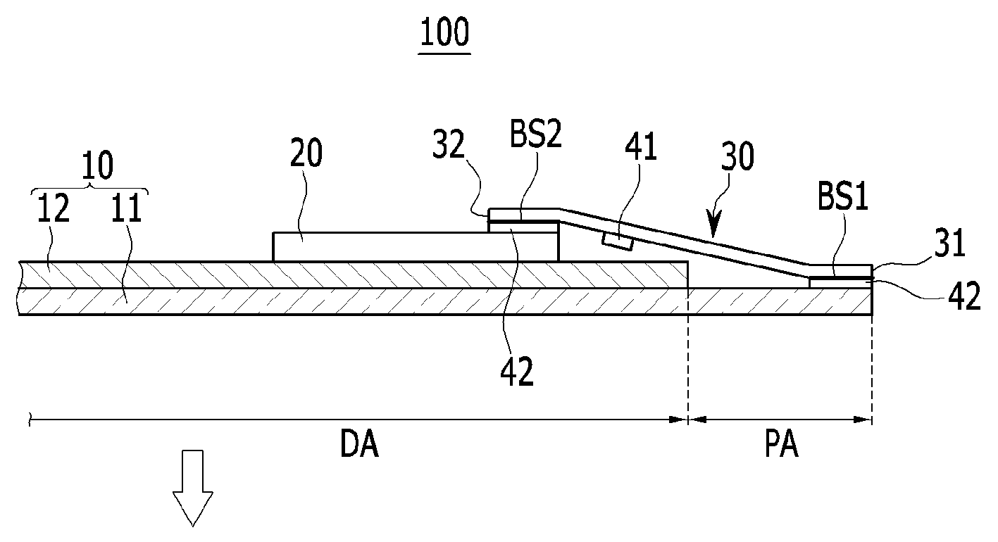
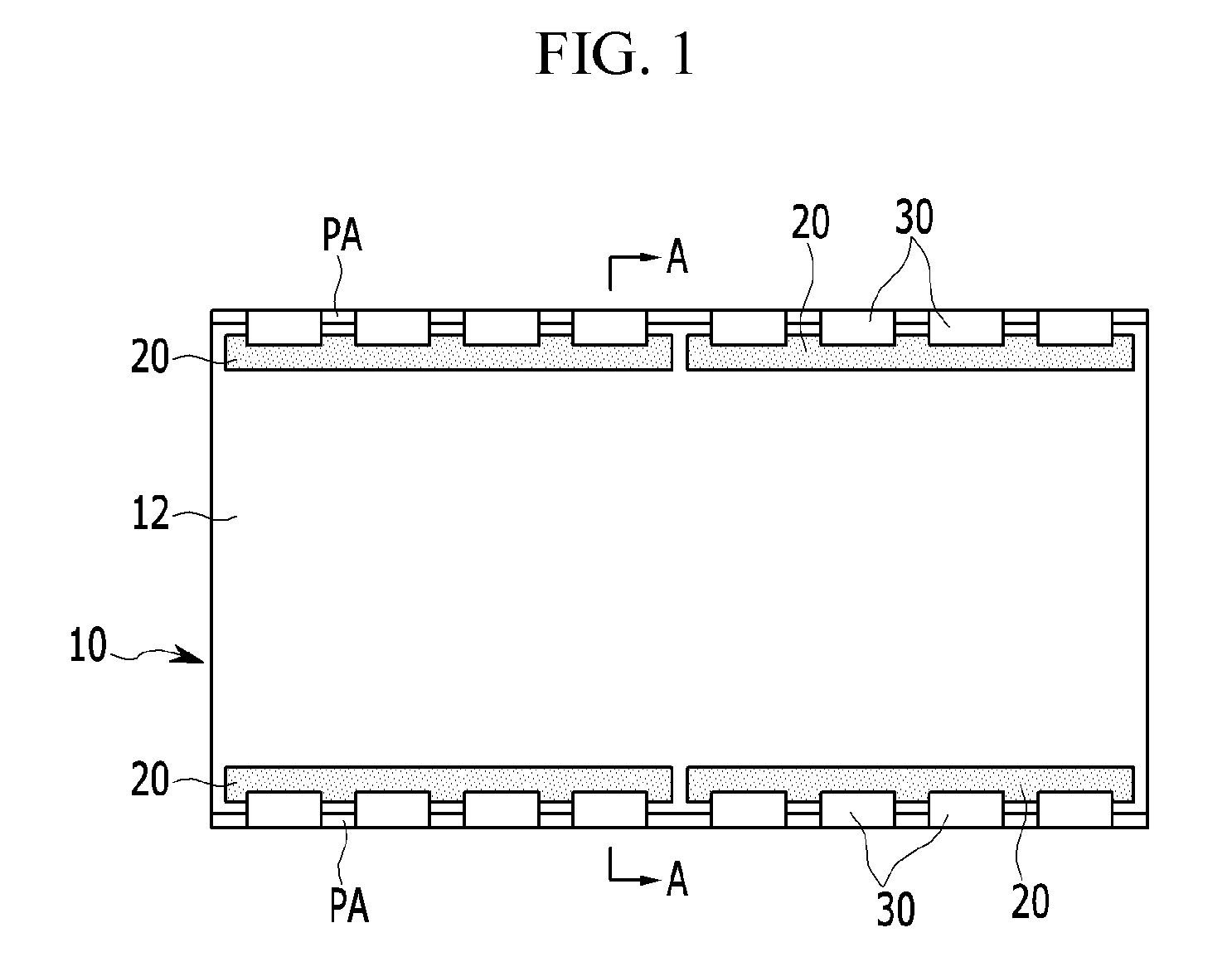
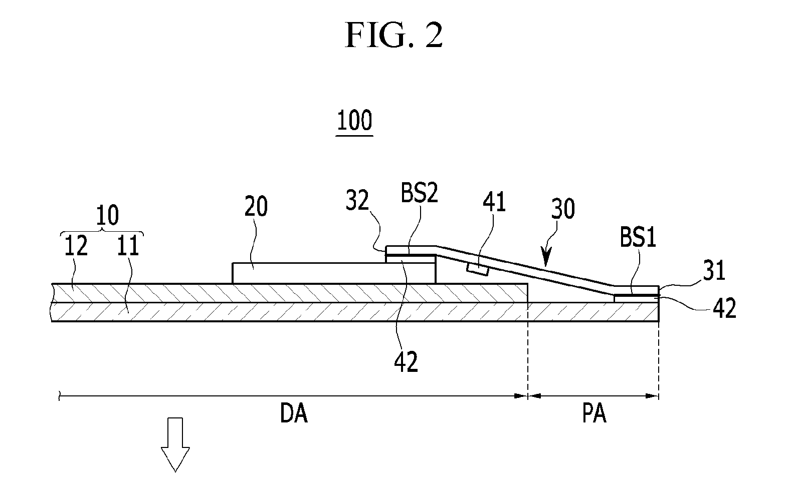
[0011]The present invention provides an organic light emitting diode (OLED) display improving an adhesion structure of a circuit film and a flexible printed circuit (FPC) to increase adhesion reliability of a circuit film and to reduce a dead space, and a manufacturing method thereof. Also, the present invention provides a rotating device of a circuit film used in a manufacturing process of an organic light emitting diode (OLED) display.
[0021]The circuit film of the organic light emitting diode (OLED) display is attached to the substrate and is not bent such that adhesion reliability deterioration such as adherence weakness or moisture penetration is not generated and it is not protruded outside the display panel such that the dead space may be reduced. In the manufacturing process of the organic light emitting diode (OLED) display, the sufficient space where the display panel is not interfered with under the second end portion of the circuit film by the rotating device is provided such that the bonding work of the circuit film and the flexible printed circuit (FPC) may be easily performed.

Problems solved by technology

In the above-described structure, the circuit film is attached to the substrate and then is bent such that adherence with the substrate becomes weak and moisture penetrates into an adhesion portion with the substrate, and thereby adhesion reliability may deteriorate.

Method used


Image

  • Organic light emitting diode display, manufacturing method thereof, and rotating device for circuit film
  • Organic light emitting diode display, manufacturing method thereof, and rotating device for circuit film
  • Organic light emitting diode display, manufacturing method thereof, and rotating device for circuit film

Examples


Embodiment Construction

[0031]The present invention will be described more fully hereinafter with reference to the accompanying drawings, in which exemplary embodiments of the invention are shown. As those skilled in the art would realize, the described embodiments may be modified in various different ways, all without departing from the spirit or scope of the present invention.

[0032]Unless explicitly described to the contrary, the word “comprise” and variations such as “comprises” and “comprising” will be understood to imply the inclusion of stated elements but not the exclusion of any other elements. In addition, it will be understood that when an element such as a layer, film, region, or substrate is referred to as being “on” another element, it can be directly on the other element or intervening elements may also be present. Throughout this specification, it is understood that the term “on” and similar terms are used generally and are not necessarily related to a gravitational reference.

[0033]FIG. 1 is...


PUM


Abstract

A manufacturing method of an organic light emitting diode (OLED) display includes: supplying a circuit film on the pad area of the display panel and bonding a first end portion of the circuit film to the pad area; vertically standing and inserting the display panel in a bonding device; holding a portion of the circuit film including a second end portion to be horizontal by using a rotating device including a vacuum absorbing portion; supplying a flexible printed circuit (FPC) into a space under the second end portion of the circuit film, and attaching the flexible printed circuit to the second end portion of the circuit film; and operating the rotating device to move the second end portion to a vertical position, and separating the circuit film from the vacuum absorbing portion.

Description

CLAIM OF PRIORITY[0001]This application claims priority to and the benefit of Korean Patent Application No. 10-2012-0114826 filed in the Korean Intellectual Property Office on Oct. 16, 2012, the entire contents of which are incorporated herein by reference.BACKGROUND OF THE INVENTION[0002]1. Field of the Invention[0003]The described technology relates generally to an organic light emitting diode (OLED) display. More particularly, the described technology relates generally to an organic light emitting diode (OLED) display including a circuit film and a flexible printed circuit (FPC), a manufacturing method thereof, and a rotating device of a circuit film used in a manufacturing process of the organic light emitting diode (OLED) display.[0004]2. Description of the Related Art[0005]Unlike the liquid crystal display (LCD), an organic light emitting diode (OLED) display does not require a separate light source, thereby making it possible to be implemented as a slim and lightweight displa...

Claims


Application Information

Patent Timeline
Patent Type & Authority Patents(United States)
IPC IPC(8): H01L29/08H01L29/786H01L27/32H01L29/18H01L29/04
CPCH01L27/3244H01L27/3276H01L2924/0002H10K59/131H01L2924/00H10K71/00H10K50/84H10K59/12H10K59/1201H10K2102/311H01L25/18H01L25/50
Inventor JUNG, HAE-GOORYU, DO-HYUNG
Owner SAMSUNG DISPLAY CO LTD
Why Eureka
Try Eureka