Method for manufacturing three dimensional stacked semiconductor structure and structure manufactured by the same

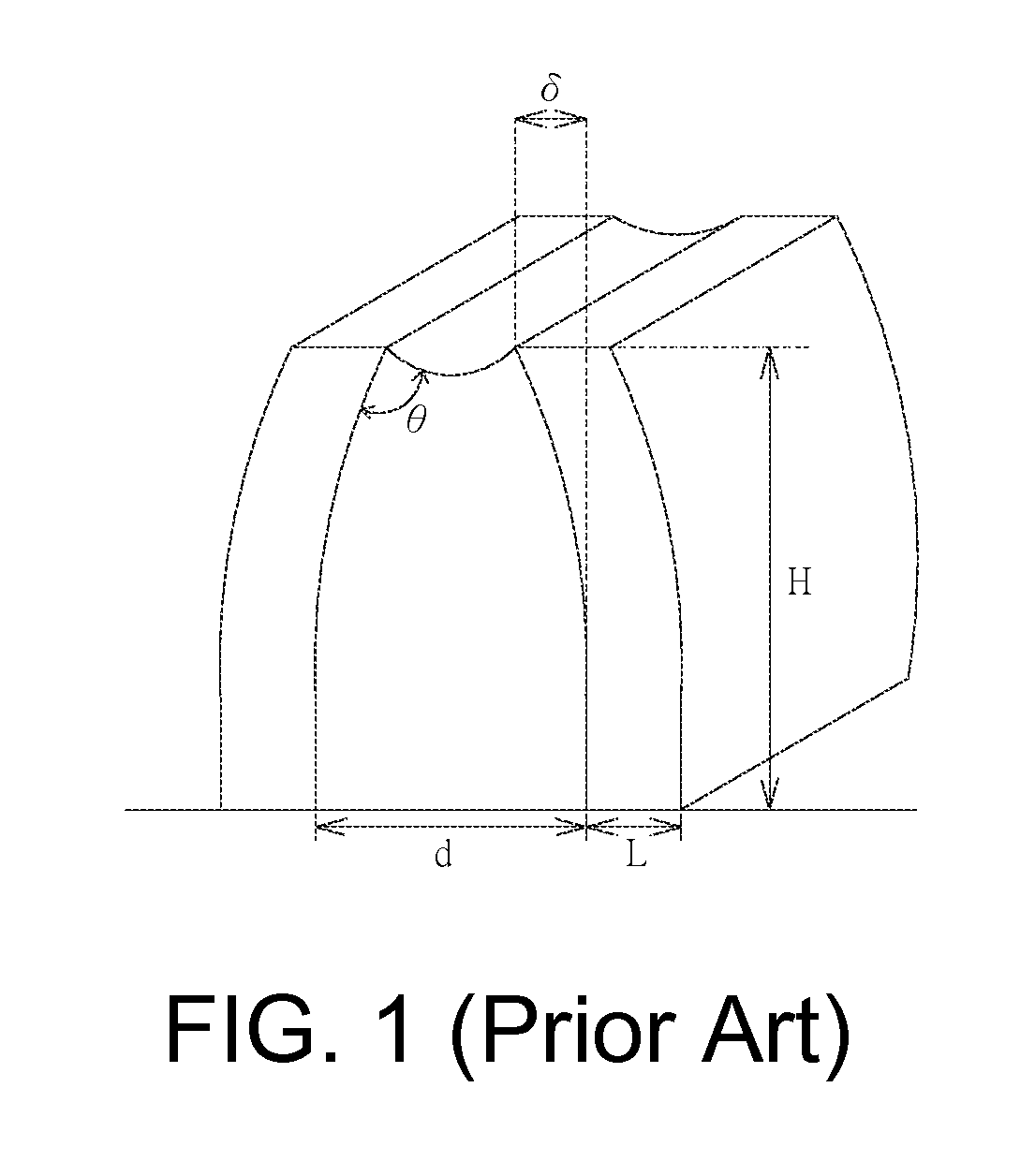
a three-dimensional stacked semiconductor and manufacturing method technology, applied in the direction of semiconductors, electrical devices, transistors, etc., can solve the problems of easy bended or collapsed problems, and the typical 3d memory structure suffers from several problems, and achieves reliable electrical characteristics.

Active Publication Date: 2015-12-01
MACRONIX INT CO LTD
View PDF4 Cites 0 Cited by
  • Summary
  • Abstract
  • Description
  • Claims
  • Application Information

AI Technical Summary

Benefits of technology

[0008]The disclosure relates to a method of manufacturing a three-dimensional (3D) stacked semiconductor structure and a structure manufactured by the same. According to the method of the embodiment, a multi-layer comprising plural first dielectric layers (compressive) and second dielectric layers (tensile) arranged alternately is formed and followed by patterning steps. The method of the embodiment solves easy-to-bended and / or collapsed problem occurring in the stacking and patterning procedures for manufacturing the conventional stacked semiconductor structure. According to the structure of the embodiment, a dielectric support Sd is formed between two adjacent multi-layered pillars for strengthening the overall construction, thereby providing a self-aligned profile and the reliable electrical characteristics.

Problems solved by technology

However, the typical 3D memory structure suffers from several problems.
For the conventional 3D stacked semiconductor structure and manufacturing method, the easily bended or collapsed problems occurred often due to higher aspect ratio. FIG. 1 schematically shows the bended pillars occurred in the conventional 3D stacked semiconductor structure.
If the pillars of the 3D stacked semiconductor structure are tall and narrow, it is easily bended or collapsed.
Also, the multi-layered pillars of the 3D stacked semiconductor structure are oxide-and-polysilicon (O-P) stacks, which exhibit unbalanced stress, and are easily collapsed or bended during manufacturing processes.

Method used


Image

  • Method for manufacturing three dimensional stacked semiconductor structure and structure manufactured by the same
  • Method for manufacturing three dimensional stacked semiconductor structure and structure manufactured by the same
  • Method for manufacturing three dimensional stacked semiconductor structure and structure manufactured by the same

Examples


Embodiment Construction

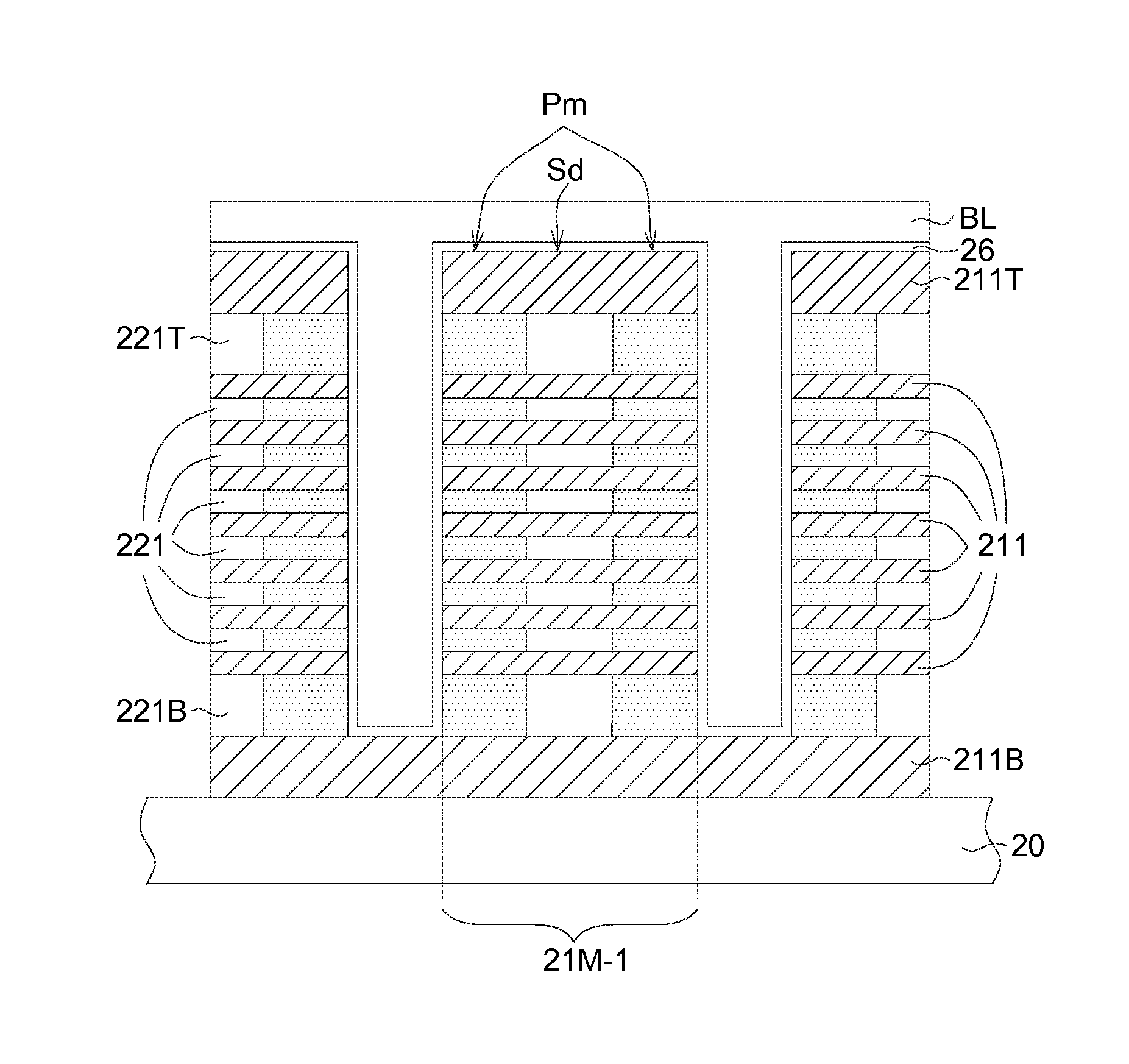
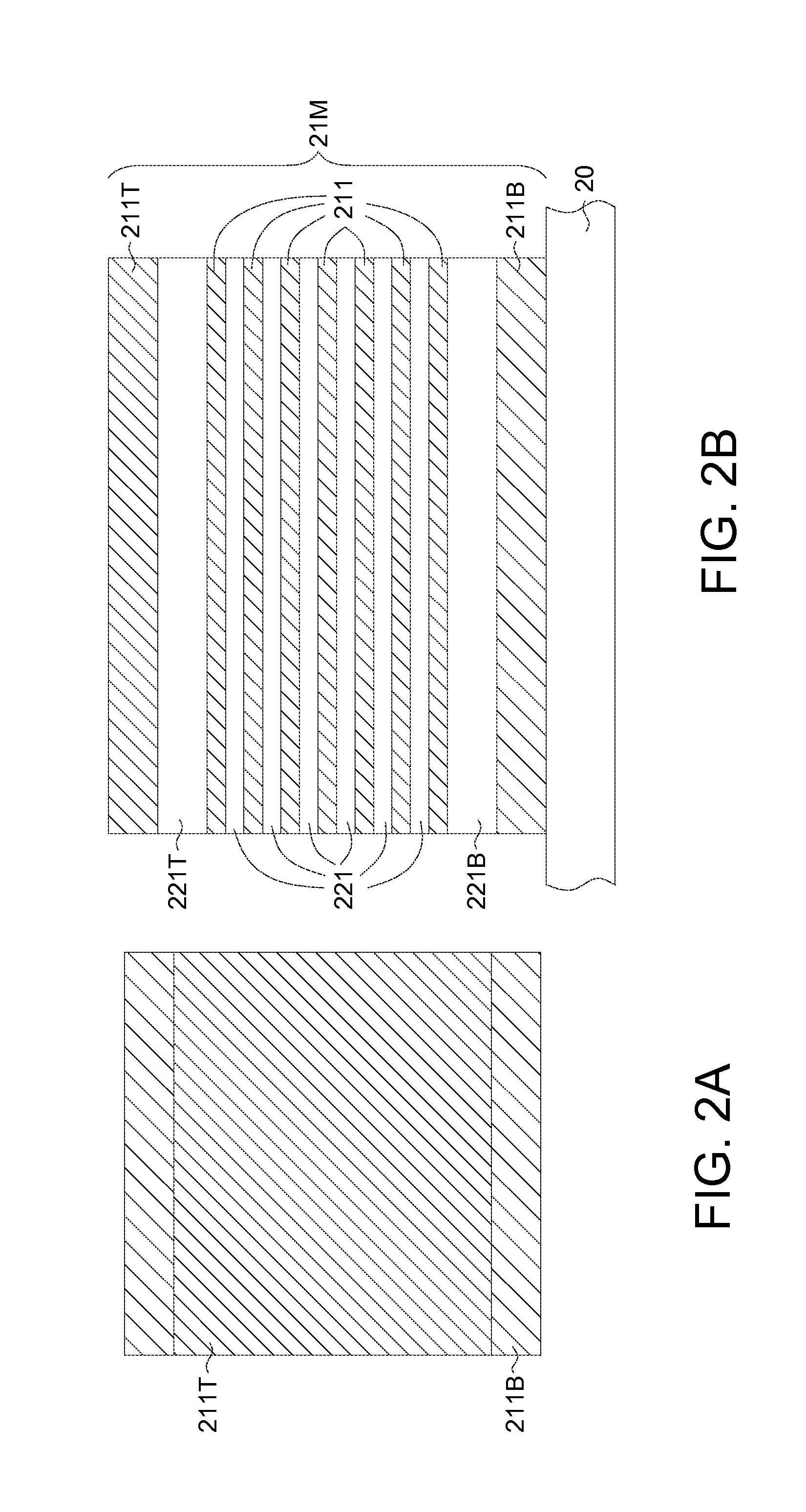
[0021]In the embodiments of the present disclosure, a method of manufacturing a three-dimensional (3D) stacked semiconductor structure and a structure manufactured by the same are provided. According to the method of the embodiment, a multi-layer comprising a plurality of first and second dielectric layers arranged alternately are formed on a substrate, followed by patterning the multi-layer to form a plurality of first patterned stacks and spaces between the first patterned stacks. According to the embodiment, the first dielectric layers are compressive layers exhibiting compressive stress, and the second dielectric layers are tensile layers exhibiting tensile stress. Parts of the second dielectric layers of one of the first patterned stacks are then replaced by conductors. The 3D stacked semiconductor structure manufactured by the method of the embodiment has plural multi-layered patterned stacks and spaces between the multi-layered patterned stacks, and each patterned stack compr...


PUM


Abstract

A method of manufacturing a three-dimensional (3D) stacked semiconductor structure is provided, comprising. A multi-layer on a substrate is formed, and the multi-layer comprises plural first dielectric layers and second dielectric layers arranged alternately. The multi-layer is then patterned to form plural first patterned stacks and spaces between the first patterned stacks, wherein one of the first patterned stacks has a width of F0 while the one of the spaces has a width of Fs. In one embodiment, F0 is equal to or more than 2 times Fs. Parts of the second dielectric layers of one of the first patterned stacks are removed, so as to form plural first cavities in the first patterned stack. Then, the first cavities in the first patterned stack are filled with conductors.

Description

BACKGROUND[0001]1. Field of the Invention[0002]The disclosure relates in general to a method of manufacturing a three-dimensional (3D) stacked semiconductor structure and a structure manufactured by the same, and more particularly to the method for manufacturing the structure having dielectric supports for multi-layered pillars, thereby strengthening the overall construction.[0003]2. Description of the Related Art[0004]A nonvolatile semiconductor memory device is typically designed to securely hold data even when power is lost or removed from the memory device. Various types of nonvolatile memory devices have been proposed in the related art. Also, manufactures have been looking for new developments or techniques combination for stacking multiple planes of memory cells, so as to achieve greater storage capacity. For example, several types of multi-layer stackable NAND-type flash memory structures have been proposed. However, the typical 3D memory structure suffers from several probl...

Claims


Application Information

Patent Timeline
Patent Type & Authority Patents(United States)
IPC IPC(8): H01L21/3205H01L27/115H01L27/108
CPCH01L27/11582H01L27/11578H01L27/10844H10B43/27H10B43/20H10B12/01
Inventor LAI, ERH-KUN
Owner MACRONIX INT CO LTD
Why Eureka
Try Eureka