Time-of-flight imaging systems

a technology of imaging system and time-of-flight, applied in the field of imaging devices, can solve the problems of long time-of-flight, confusion of range finding system based on the brightness of reflected light, and difficulty in separating background intensity from reflected light pulse intensity,

Active Publication Date: 2016-01-05
SEMICON COMPONENTS IND LLC
View PDF1 Cites 4 Cited by
  • Summary
  • Abstract
  • Description
  • Claims
  • Application Information

AI Technical Summary

Benefits of technology

[0008]Various embodiments are described, illustrating electronic devices that include time-of-flight image pixels configured to measure the time of flight of an emitted light pulse for sensing distance information about objects in a scene. Emitted light pulses may be generated by a light pulse emitter on the electronic device and reflected from objects in the field-of-view of the time-of-flight image pixels. Time-of-flight image pixels may be configured to measure differences in time-of-flight between reflected portions of emitted light pulses using differences in brightness of the reflected portions. Time-of-flight image sensors may be configured to remove background light contamination of reflected portions of emitted light pulses.

Problems solved by technology

This is because the light reflected from the far away object travels a longer distance and therefore has a longer time-of-flight.
However, range finding systems of this type typically collect distance information for a single point, not a collection of points as in an image.
In addition, range finding systems that determine depth information based on the brightness of reflected light may be confused by the presence of differences in the intrinsic brightness of objects in a typical real-world scene.
Difficulties that arise in separating background intensity from reflected light pulse intensity can therefore be problematic when capturing images with depth information.

Method used


Image

  • Time-of-flight imaging systems
  • Time-of-flight imaging systems
  • Time-of-flight imaging systems

Examples


Embodiment Construction

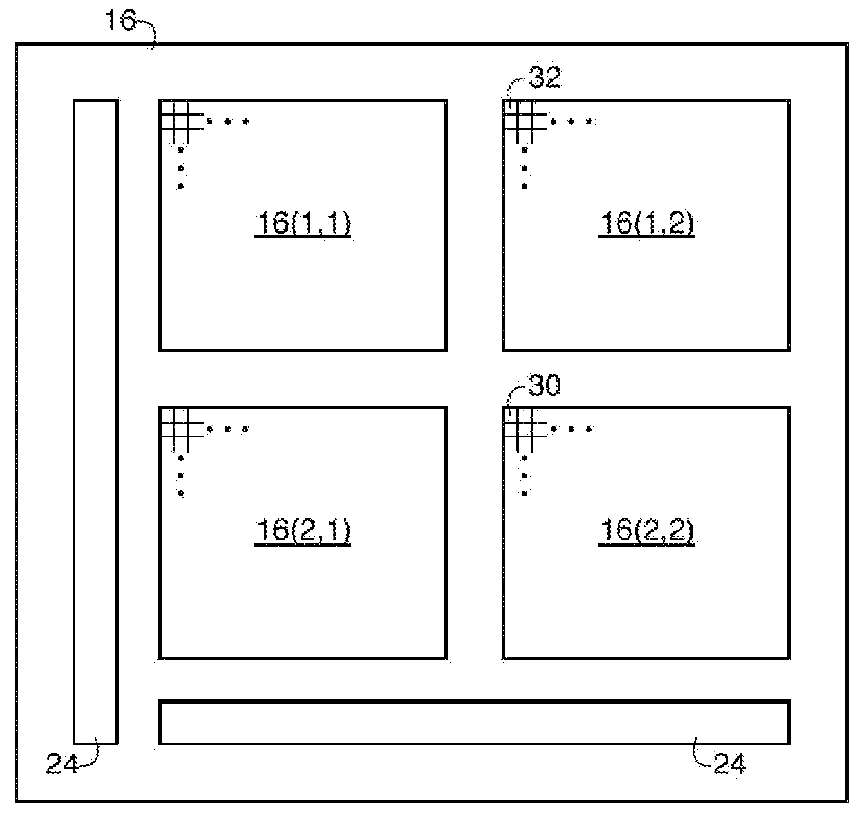
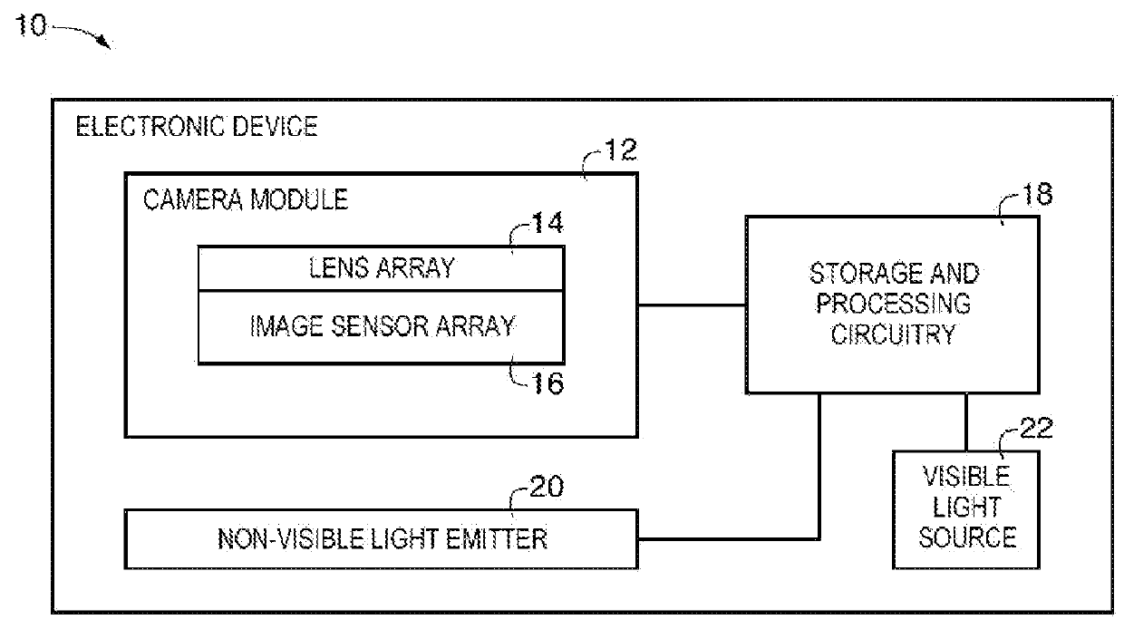
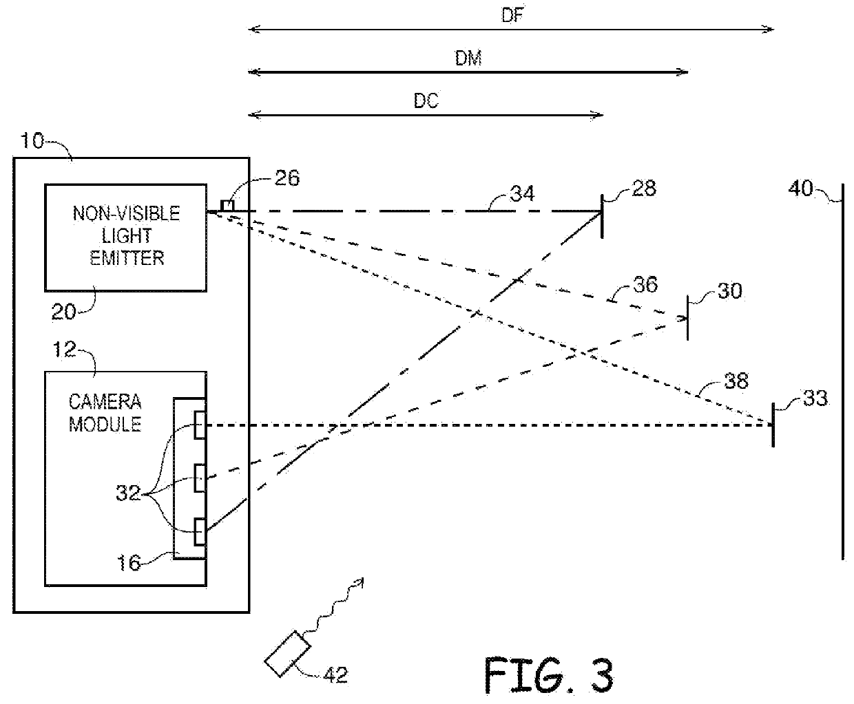
[0036]Digital camera modules are widely used in electronic devices such as digital cameras, computers, cellular telephones, or other electronic devices. These electronic devices may include image sensors that gather incoming light to capture an image. The image sensors may include arrays of image pixels. The image sensors may include arrays of time-of-flight image pixels for sensing the flight time of a light pulse emitted by a non-visible-light emitting component of the electronic device and reflected from an object. Image sensors may, if desired, include both image pixels and time-of-flight image pixels. Image pixels and time-of-flight image pixels in the image sensors may include photosensitive elements such as photodiodes that convert the incoming light into electric charges.

[0037]Time-of-flight image sensor pixels may include one or more charge storage regions for storing charges collected using photosensitive elements. Time-of-flight image sensors may be configured to store ch...


PUM


Abstract

Electronic devices may include time-of-flight image pixels. A time-of-flight image pixel may include first and second charge storage regions coupled to a photosensor and a transfer transistor with a gate terminal coupled to the first storage region. An electronic device may further include a light pulse emitter configured to emit pulses of light to be reflected by objects in a scene. Reflected portions of the emitted pulses of light may be captured along with background light by the time-of-flight image pixels. Time-of-flight image pixels may be configured sense the time-of-flight of the reflected portions of the emitted pulses. The electronic device may include processing circuitry configured to use the sensed time-of-flight of the reflected portions to generate depth images of a scene. Depth images may include depth-image pixel values that contain information corresponding to the distance of the objects in the scene from the electronic device.

Description

[0001]This application claims the benefit of provisional patent application No. 61 / 512,306, filed Jul. 27, 2011, which is hereby incorporated by reference herein in its entirety.BACKGROUND[0002]This relates generally to imaging devices, and more particularly, to imaging devices that measure the flight time of reflected light pulses.[0003]Image sensors are commonly used in electronic devices such as cellular telephones, cameras, and computers to capture images. In a typical arrangement, an electronic device is provided with an image sensor and a corresponding lens. Some electronic devices use arrays of image sensors and corresponding lenses to gather image data. This type of system, which is sometimes referred to as an array camera, may be used to capture depth information from a scene using a parallax effect based on a known physical offset between image sensors.[0004]Depth information such as information about the distance of an object from an electronic device is also commonly cap...

Claims


Application Information

Patent Timeline
Patent Type & Authority Patents(United States)
IPC IPC(8): H01L31/16G01S7/486H04N5/232G01S17/89H04N5/225H04N13/02H04N5/3745H04N5/359H01L27/148G01J1/44G01J1/42G01S7/4863G01S17/894
CPCG01S7/4863G01S17/89H01L31/165H04N5/2258H04N5/2327G01J2001/4238G01J2001/444G01N2201/0696H01L27/148H04N5/359H04N5/37452H04N13/0253H04N13/254G01S17/894H04N25/62H04N25/771H04N23/45H04N23/684
Inventor KIM, DONGSOOLIM, JAE EUNCHO, KWANGBO
Owner SEMICON COMPONENTS IND LLC
Why Eureka
Try Eureka