Semiconductor device having high mobility channel
- Summary
- Abstract
- Description
- Claims
- Application Information
AI Technical Summary
Benefits of technology
Problems solved by technology
Method used
Image
Examples
Embodiment Construction
[0035]Particular embodiments of the present disclosure are described below with reference to the drawings. In the description, common features are designated by common reference numbers throughout the drawings.
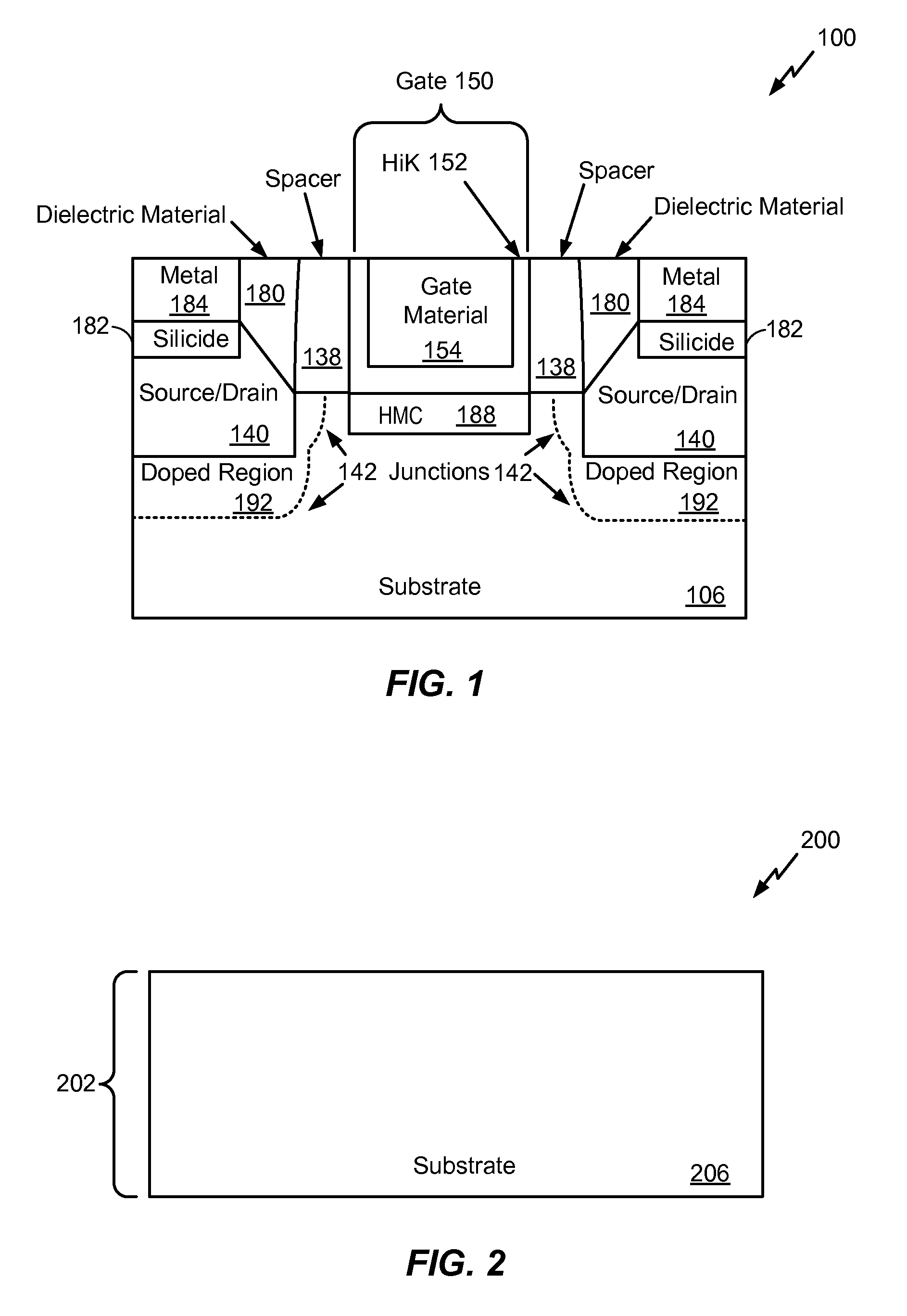
[0036]Referring to FIG. 1, a diagram of a semiconductor device 100 including a high mobility channel is shown. The semiconductor device 100 may include a complementary metal-oxide-semiconductor (CMOS) device, such as a p-type metal-oxide-semiconductor (pMOS) device or an n-type metal-oxide-semiconductor (nMOS) device.
[0037]The semiconductor device 100 includes a substrate 106, such as a silicon (Si) substrate. The substrate 106 may include source / drain (S / D) regions 140 and a high mobility channel (HMC) 188. The source / drain regions 140 (e.g., source / drain implants) may include silicon germanium (SiGe), embedded silicon (e-Si), embedded silicon carbon (e-Si:C), or silicon doped with phosphorous (Si:P). Each of the source / drain regions 140 may be associated with a corresponding...
PUM
 Abstract
Description
Claims
Application Information


