Display panel

a display panel and panel technology, applied in static indicating devices, instruments, optics, etc., can solve the problems of difficult to realize a display panel with thin borders with such a traditional approach, electronic devices becoming thinner, lighter and smaller, etc., to achieve the effect of avoiding parasitic capacitance, and reducing the cost of production

Active Publication Date: 2016-01-26
E INK HLDG INC
View PDF13 Cites 2 Cited by
  • Summary
  • Abstract
  • Description
  • Claims
  • Application Information

AI Technical Summary

Benefits of technology

[0020]In summary, with the embodiments mentioned above, the borders of the display panel can be thinner by using the first and second transmission lines to transmit the second signal. The first pins and the second pins of the driver IC chip can be evenly disposed and interleaved, so that the first signal lines and the transmission lines do not cross over each other, and the capacitance coupling effect and stray capacitance can be avoided. In addition, by ensuring that the orthogonal projections of the first signal lines, the first transmission lines, the second transmission lines, and the dummy lines on the substrate do not overlap, parasitic capacitance can be avoided. Moreover, by evenly disposing the dummy lines and the second transmission lines, load imbalance in the active area of the display panel also can be avoided, so that the quality of the image of the display panel can be improved.

Problems solved by technology

However, it is difficult to realize a display panel with thin borders with such a traditional approach, and this runs counter to trends of making electronic devices increasingly thinner, lighter and smaller.

Method used


Image

  • Display panel
  • Display panel
  • Display panel

Examples


Embodiment Construction

[0028]In the following detailed description, for purposes of explanation, numerous specific details are set forth in order to attain a thorough understanding of the disclosed embodiments. It will be apparent, however, that one or more embodiments may be practiced without these specific details. In other instances, well-known structures and devices are schematically shown in order to simplify the drawing.

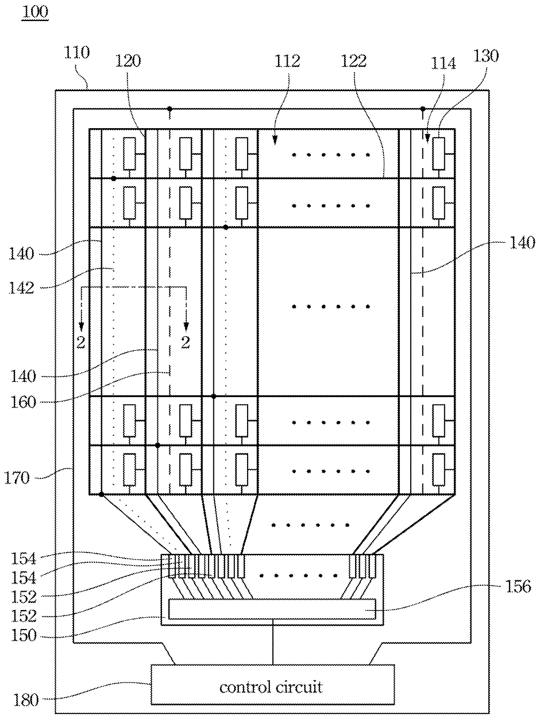
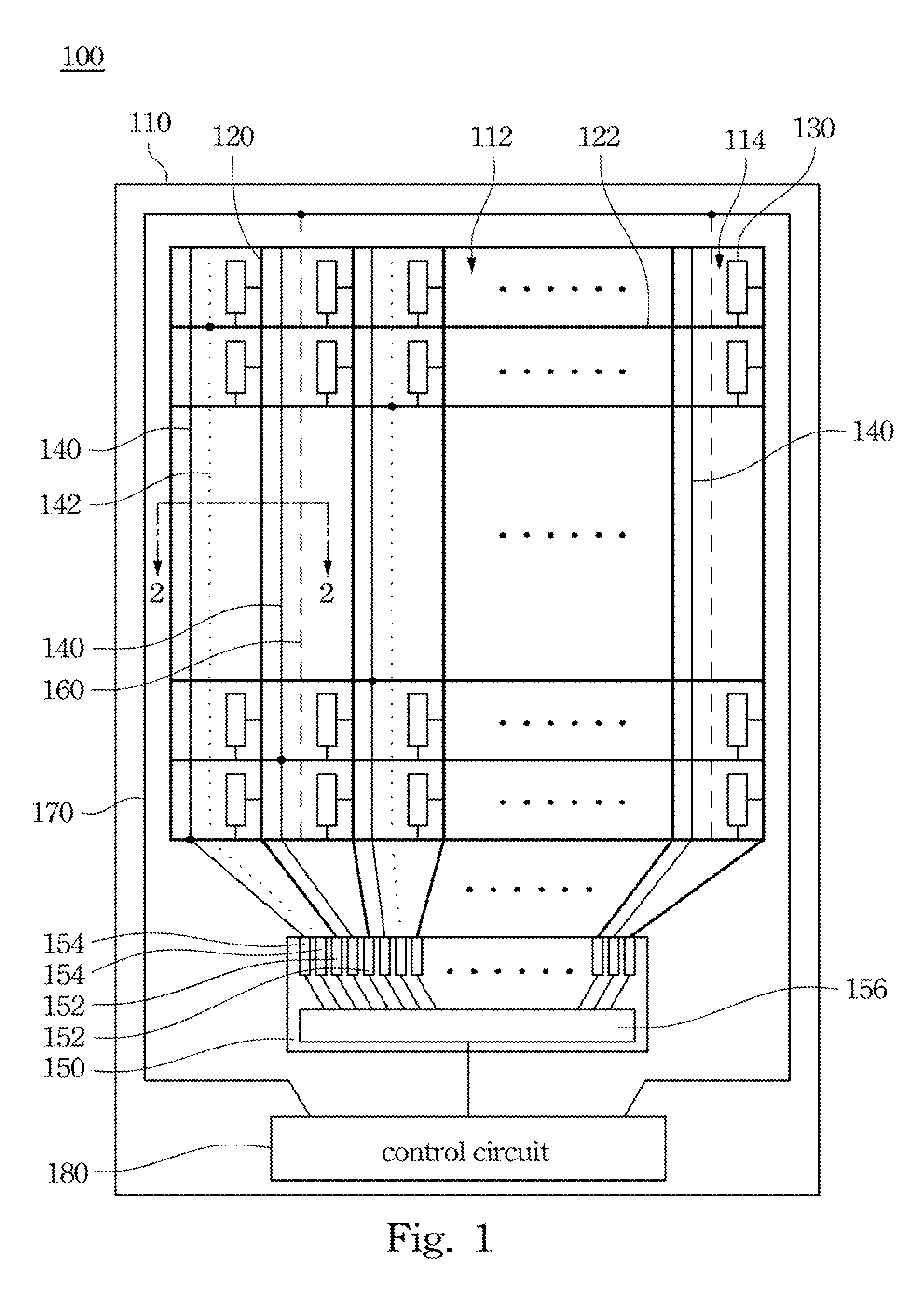
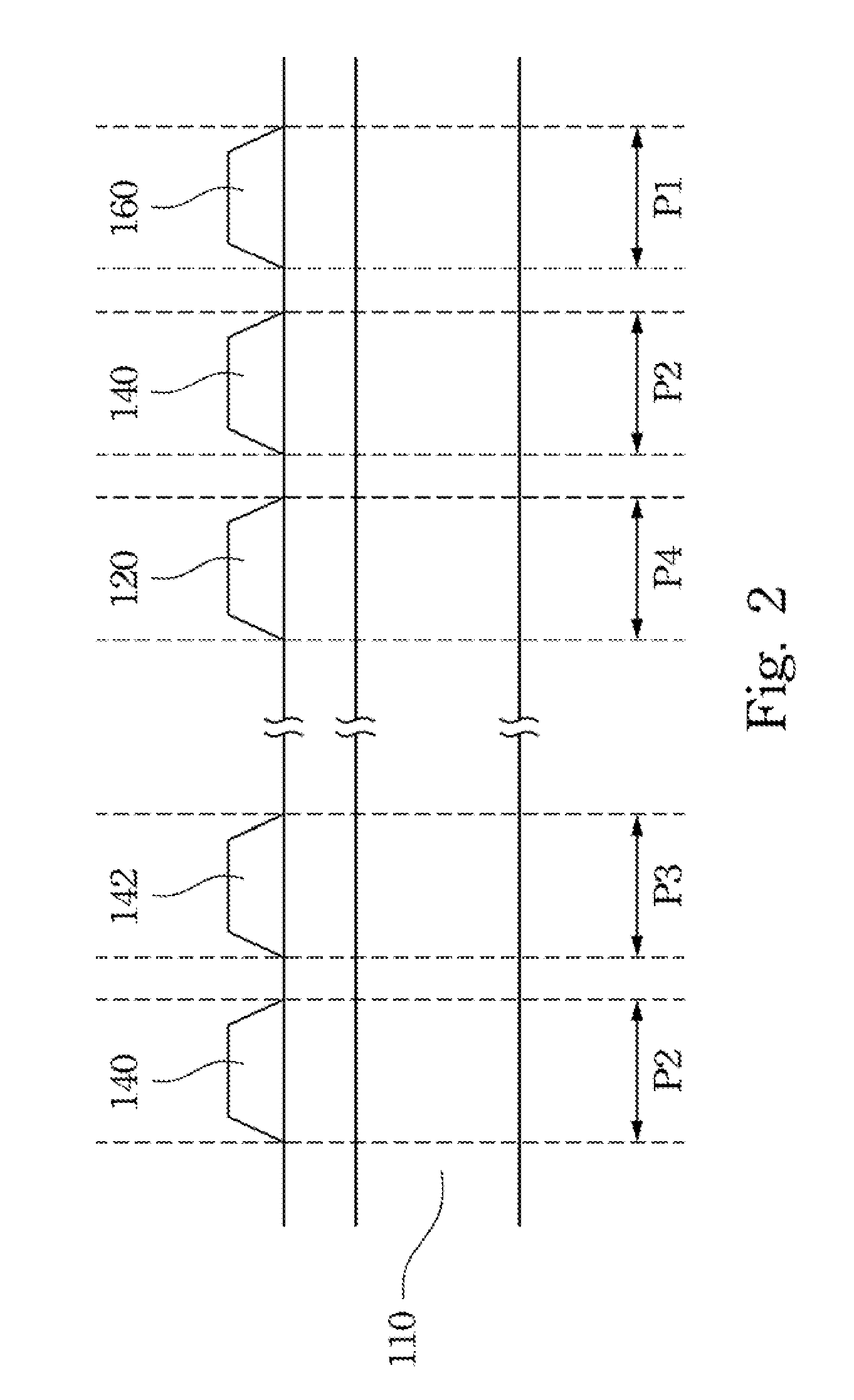
[0029]FIG. 1 is a schematic diagram of a display panel 100 in accordance with one embodiment of the present disclosure. The display panel 100 includes a substrate 110, a plurality of first signal lines 120, a plurality of second signal lines 122, a plurality of pixel units 130, a plurality of transmission lines 140, 142, and a driver IC chip 150. It is noted that the first signal lines 120 and the second to signal lines 122 may separately be data lines and scan lines. That is, when the first signal lines 120 are data lines, the second signal lines 122 are the scan lines, and vice ver...


PUM

PropertyMeasurementUnit
voltage levelaaaaaaaaaa

Abstract

A display panel includes a substrate, a plurality of first signal lines, a plurality of second signal lines, a plurality of pixel units, a plurality of transmitting lines, and a driving chip. The transmitting lines are disposed on the substrate and electrically connected to the second signal lines. The driving chip includes a plurality of first pins, a plurality of second pins, and a driving circuit. The first pins are electrically connected to the first signal lines, and the second pins are electrically connected to the transmitting lines. The first pins and the second pins are disposed alternately and evenly, such that the first signal lines and the transmitting lines do not intersect each other. The transmitting lines are disposed on the substrate evenly.

Description

RELATED APPLICATIONS[0001]This application claims priority to U.S. Provisional Application Ser. No. 61 / 587,643, filed Jan. 17, 2012, and Taiwan Application Serial Number 101123897, filed Jul. 3, 2012, the disclosures of which are incorporated herein by reference in their entireties.BACKGROUND[0002]1. Field of Invention[0003]The present disclosure relates to display technology. More particularly, the present invention relates to a display panel.[0004]2. Description of Related Art[0005]With advances in display technology, display panels have been used in various different electronic products, such as cell phones, tablet computers, and digital cameras.[0006]A display panel typically has a scan IC chip and a data IC chip disposed respectively to two sides of an active area. Wiring lines are disposed around the active area for providing signals to scan lines and data lines orthogonal to the scan lines. With such a configuration, a sufficient space is necessary around the active area to p...

Claims


Application Information

Patent Timeline
Patent Type & Authority Patents(United States)
IPC IPC(8): G02F1/1343H05B37/00H01L27/32G02F1/1345
CPCH05B37/00G02F1/1343G02F1/1345H01L27/3276G02F2001/13456G09G2300/0426G02F1/13456H10K59/131G09G3/32H01L27/124
Inventor CHANG, SHU-HAOWU, CHI-MINGFRENCH, IAN
Owner E INK HLDG INC
Why Eureka
Try Eureka