Display device having resin layer

a liquid crystal display and resin layer technology, applied in semiconductor devices, instruments, optics, etc., can solve the problems of negligible black matrix capacitance and interlayer insulating film capacitance, and achieve the effect of reducing overlap width and improving bonding accuracy

Inactive Publication Date: 2005-09-22
SEMICON ENERGY LAB CO LTD
View PDF54 Cites 12 Cited by
  • Summary
  • Abstract
  • Description
  • Claims
  • Application Information

AI Technical Summary

Benefits of technology

[0015] To solve the above two problems, an object of the present invention is to form a black matrix on TFTs of a driver circuit. This configuration has an advantage that the overlapping width can be reduced to about 2 μm because of improved bonding accuracy that is obtained by forming the black matrix and the ITO pixel electrodes on the same substrate.
[0021] It is now desired to provide a liquid crystal display device which enables light shielding of driver circuit regions without increasing the number of manufacturing steps.
[0022] Another object of the invention is to prevent a capacitance from occurring in an interlayer insulating film formed between TFTs of a driver circuit and a black matrix, to reduce, in turn, the delay time of the driver circuit, to thereby produce high-resolution images.
[0028] Where thin-film transistors (hereinafter called TFTs) are formed on a substrate, it is preferred to use a no-alkali glass substrate or a quartz substrate. Where it is intended to reduce the weight of a liquid crystal panel, there may be used a film that is low in birefringence, such as PES (polyethylene sulfate).
[0035] Among the above processes, the method of dispersing carbon black in an acrylic resin is preferred because it can reduce the resistance and form a thin film.
[0039] The liquid crystal material may be a nematic, cholesteric, or smectic material, or a dispersive liquid crystal in which one of those materials is dispersed in a transparent resin material. In particular, because the dispersive liquid crystal does not require the use of a polarizing plate, it can provide a bright panel.

Problems solved by technology

Where the black matrix for light shielding of the pixel region is formed on the substrate on which TFTs are formed and is also used for light shielding of the driver circuits to satisfy the above requirement, there has occurred a problem that the capacitance of an interlayer insulating film between TFTs of the driver circuits and the black matrix is not negligible though the shielding itself does not cause any problem.

Method used


Image

  • Display device having resin layer
  • Display device having resin layer
  • Display device having resin layer

Examples


embodiment 1

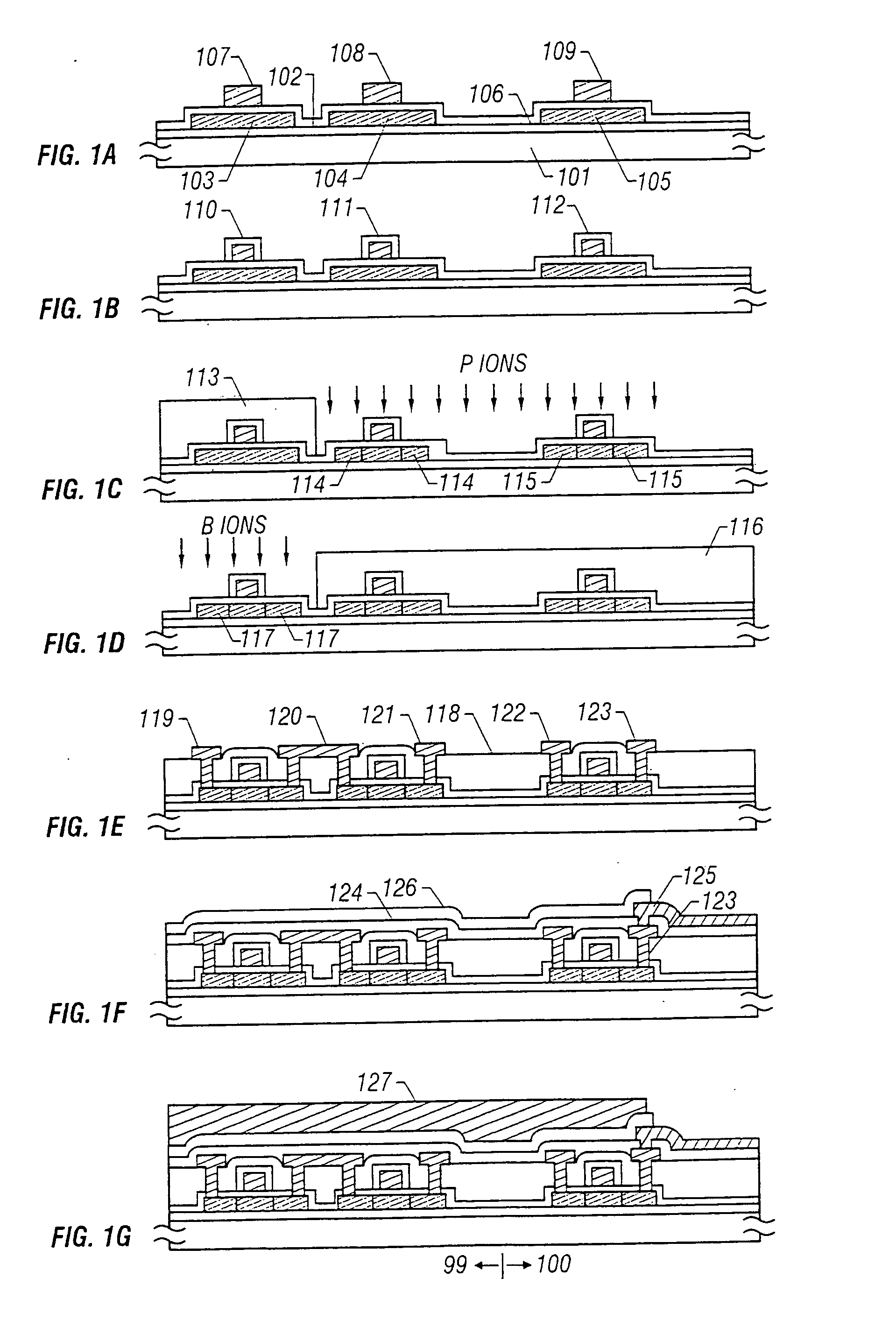
[0054] Referring to FIGS. 1A-1G, a description is made of a manufacturing process of a monolithic active matrix circuit according to a first embodiment of the invention. This is a low-temperature polysilicon process. In FIGS. 1A-1G, the left side shows a manufacturing process of TFTs 99 of a driver circuit and the right side shows a manufacturing process of a TFT 100 of an active matrix circuit.

[0055] First, a silicon oxide film of 1,000-3,000 Å in thickness, i.e., an undercoat oxide film 102 is formed on a glass substrate 101 (first insulating substrate) by sputtering or plasma CVD in an oxygen atmosphere.

[0056] Then, an amorphous silicon film having a thickness of 300-1,500 Å, preferably 500-1,000 Å, is formed by plasma CVD or LPCVD, and crystallized or improved in crystallinity by thermal annealing at a temperature not lower than 500° C., preferably 500-600° C. Optical annealing (for instance, laser annealing) may be performed after the thermal annealing to further improve the ...

embodiment 2

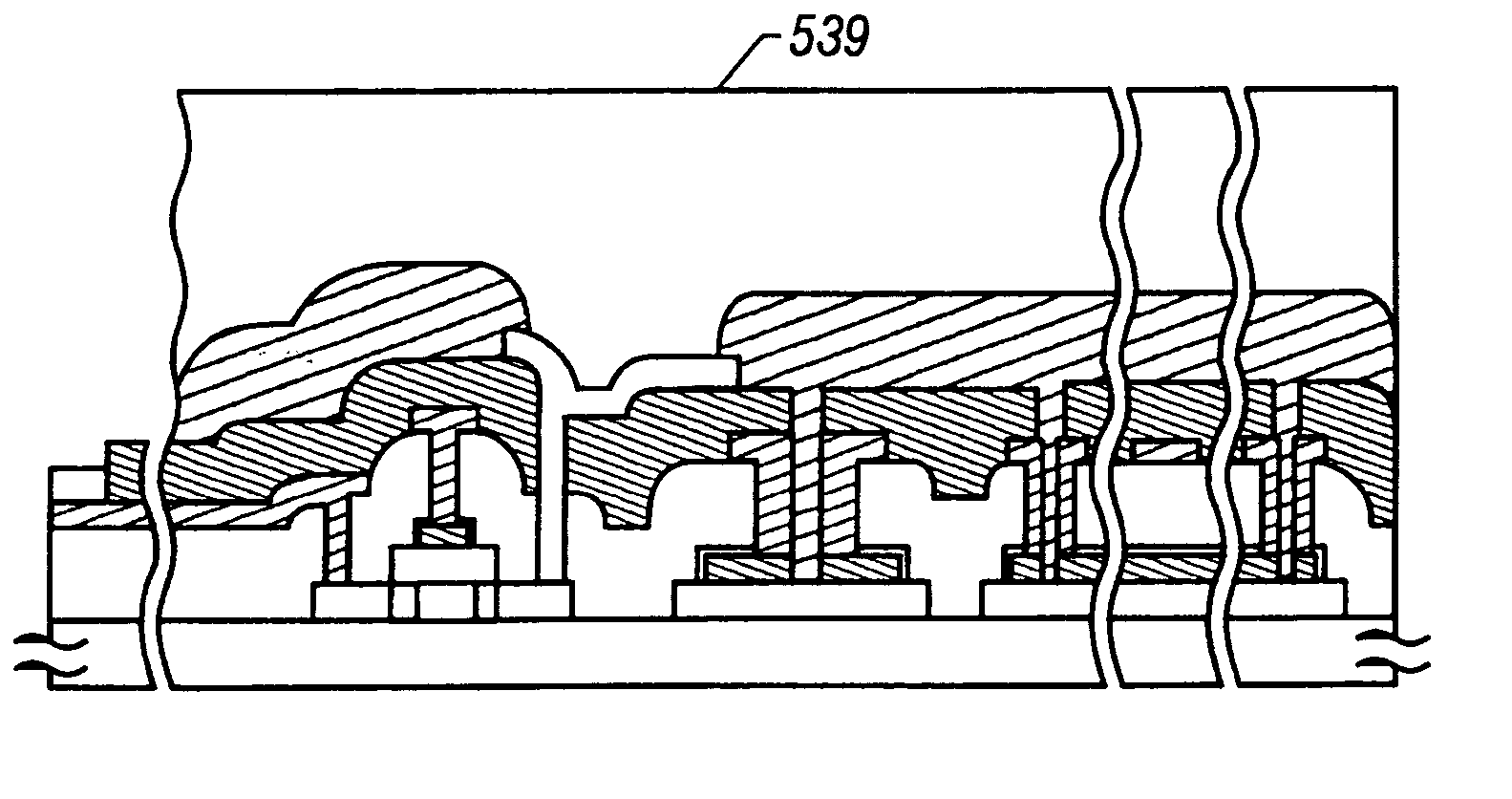
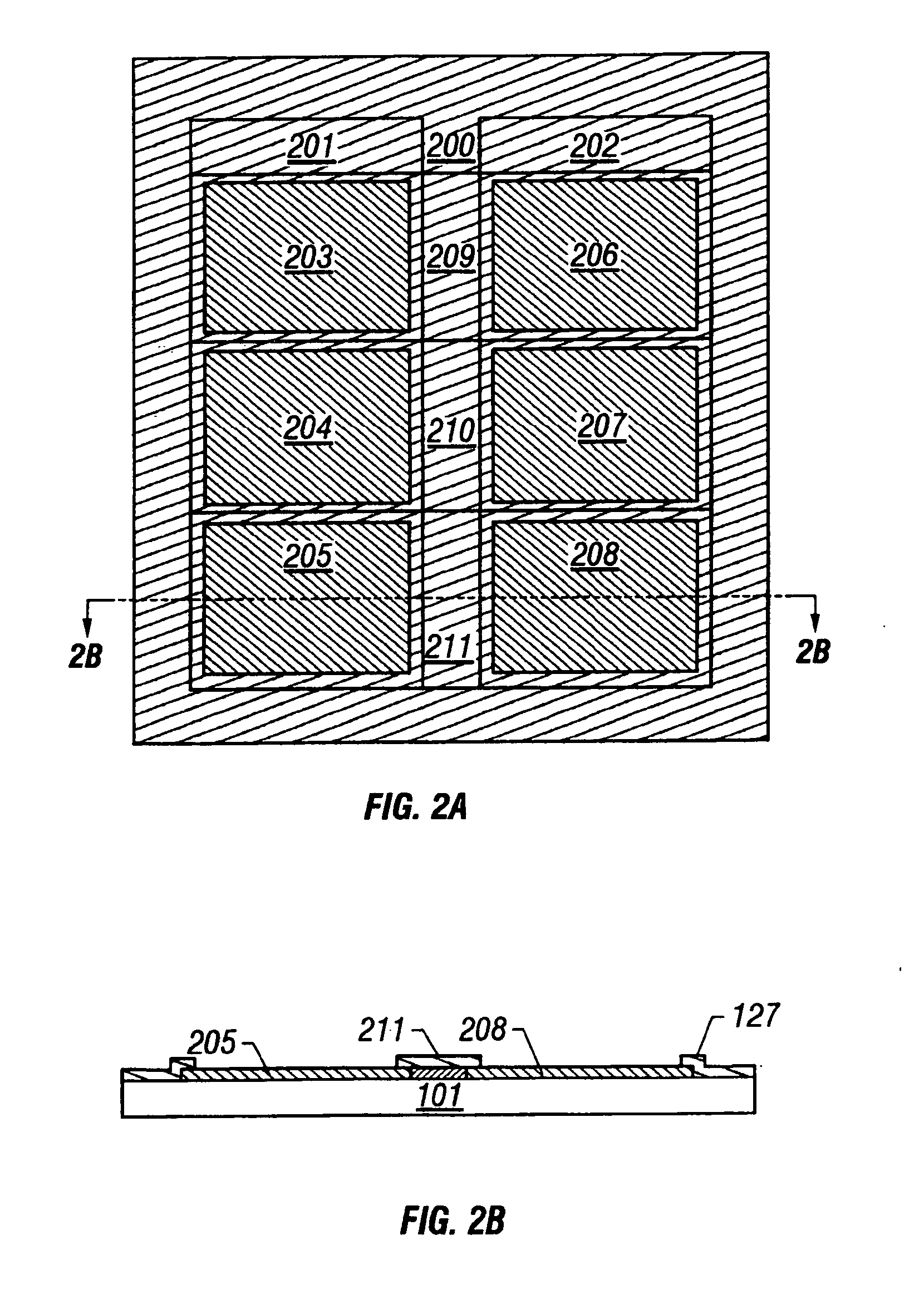
[0069] This embodiment is directed to the configuration of an integrated liquid crystal panel which is formed according to the manufacturing method of the first embodiment and in which six panels are unified. FIGS. 2A and 2B show a general configuration of an integrated liquid crystal panel according to this embodiment.

[0070]FIG. 2A is a plan view of the integrated liquid crystal panel and shows a general configuration of a substrate on which TFTs are formed. FIG. 2B is a sectional view taken along line A-A′ in FIG. 2A. FIGS. 2A and 2B show a state in which the resin black matrix 127 of the first embodiment is formed in peripheral driver circuits 201, 202 and 209-211.

[0071] In the peripheral driver circuits, because of a high degree of integration, such defects as reduce the production yield occur at a high possibility. According to an empirical rule in forming an integrated circuit, the yield is lower in a peripheral portion of a substrate than in its central portion. This is con...

embodiment 3

[0074] This embodiment is directed to a case where a planation film is provided on a substrate according to the second embodiment on which TFTs are formed. That is, a planation film 428 is provided in a pixel region and regions where a black matrix is formed.

[0075]FIGS. 3A and 3B show this embodiment in which the same reference numerals as in the second embodiment denote the same parts.

[0076] First, a substrate according to the second embodiment formed with TFTs are produced according to the manufacturing method of the first embodiment. FIGS. 4A-4G show a specific manufacturing process.

[0077] First, a silicon oxide film of 1,000-3,000 Å in thickness, i.e., an undercoat oxide film 402 is formed on a glass substrate 401 (first insulating substrate) through sputtering or plasma CVD in an oxygen atmosphere.

[0078] Then, an amorphous silicon film having a thickness of 300-1,500 Å, preferably 500-1,000 Å, is formed by plasma CVD or LPCVD, and crystallized or improved in crystallinity b...


PUM

PropertyMeasurementUnit
capacitanceaaaaaaaaaa
widthaaaaaaaaaa
particle diameteraaaaaaaaaa

Abstract

A display device is disclosed. The display device has a first substrate having a thin film transistor connected to a pixel electrode. Further, the display device has a second substrate opposed to the first substrate and having a resin black matrix.

Description

BACKGROUND OF THE INVENTION [0001] 1. Field of the Invention [0002] The present invention relates to an active matrix liquid crystal display device. [0003] 2. Description of Related Art [0004] Active matrix liquid crystal display devices are known as being effective for high-quality display. They are constructed such that thin-film transistors are formed on a transparent substrate (usually a glass or quartz substrate) for respective pixels. Each thin-film transistor controls charge that enters or exits from an electrode (pixel electrode) of the associated pixel. The active matrix liquid crystal display devices require circuits (peripheral circuits) for driving the thin-film transistors for the respective pixels. In general, the peripheral circuits are constructed as an external IC circuit called a driver IC. [0005] In an advanced version, the peripheral circuits formed by using thin-film transistors are integrated on the substrate. Providing a unified structure in which the pixel re...

Claims


Application Information

Patent Timeline
Patent Type & Authority Applications(United States)
IPC IPC(8): G02F1/1335G02F1/136G02F1/1362
CPCG02F1/133512G02F1/136209G02F1/13454G02F1/136222
Inventor YAMAZAKI, SHUNPEINISHI, TAKESHI
Owner SEMICON ENERGY LAB CO LTD
Why Eureka
Try Eureka