Method of manufacturing MRAM memory elements
a technology of memory elements and mram, which is applied in the manufacture/treatment of galvano-magnetic devices, galvano-magnetic device details, etc., can solve the problems of generating defects, affecting the performance of mram, and difficult to form ultra-small photo-resist pillar patterns
- Summary
- Abstract
- Description
- Claims
- Application Information
AI Technical Summary
Benefits of technology
Problems solved by technology
Method used
Image

Examples
Embodiment Construction
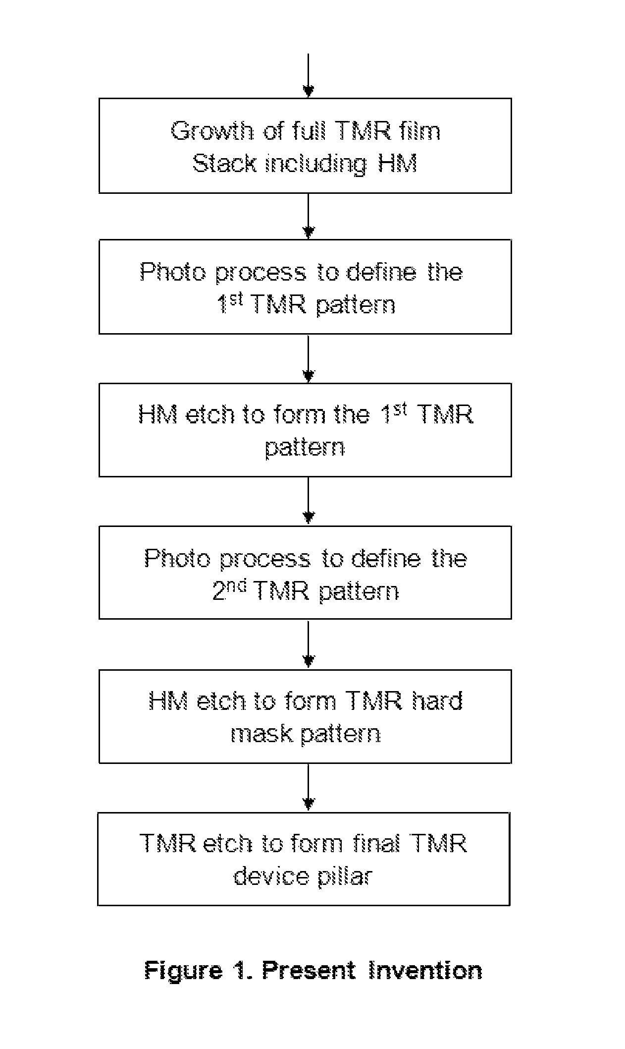
[0020]Spin transfer torque magnetic random access memory (STT-MRAM) requires small dimensions of magnetoresistive elements to be able to recording, or switch, with a small spin transfer current. Due to the limitation (such as UV light source and photo-resist thickness) of the current photolithography technology, it is extremely difficult to form ultra-small photo-resist pillar mask pattern array with a good straightness and uniformity. If the cell size is getting very small for high capacity applications, the photo-resist pillars will tilt, or bend, or even collapse before etching.
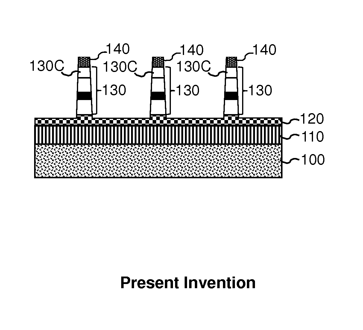
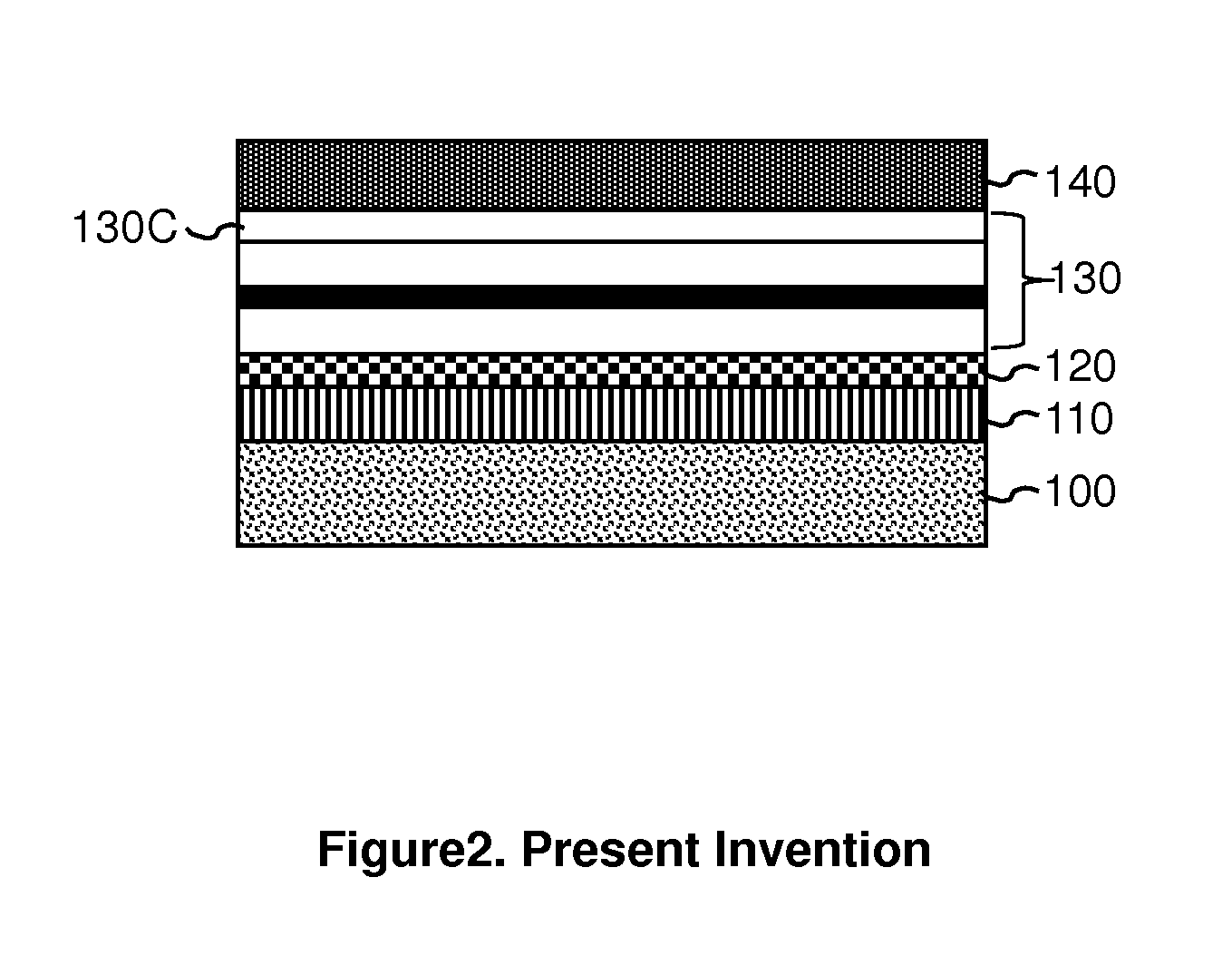
[0021]In this invention, we use dual photolithography processes to form hard mask pillar array first before etching and patterning the magnetoresistive stack into final memory element size. A process flow chart of the fabrication is as shown in FIG. 1. First, the full stack of the MRAM film layers is deposited on a substrate (100) in an ultra-high vacuum system. The film stack, as shown in FIG. 2, contains...
PUM
 Abstract
Description
Claims
Application Information