

Semiconductor device
a technology of semiconductors and semiconductors, applied in the direction of semiconductor devices, electrical devices, transistors, etc., can solve the problems of deterioration or variations in the electrical characteristics of transistors, the likely decrease of the yield of integrated circuits of miniaturized transistors, and the likely decrease of the yield of miniaturized transistors. , to achieve the effect of reducing the yield, reducing the electrical characteristics, and high degree of integration
- Summary
- Abstract
- Description
- Claims
- Application Information
AI Technical Summary
Benefits of technology
Problems solved by technology
Method used
Image

Examples
embodiment 1
[0048]In this embodiment, a semiconductor device of one embodiment of the present invention is described with reference to drawings.
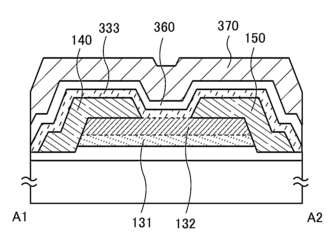
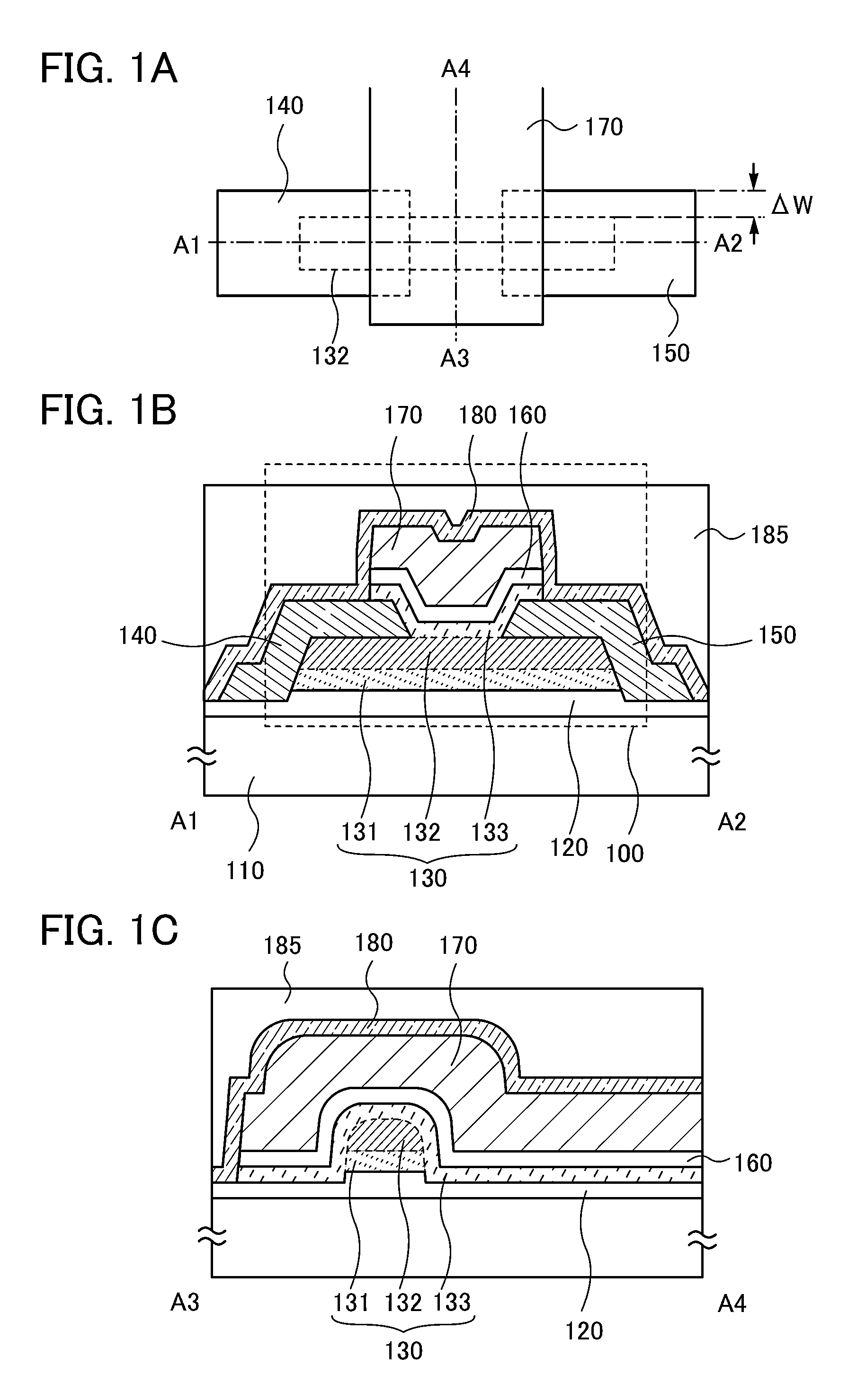
[0049]FIGS. 1A to 1C are a top view and cross-sectional views of a transistor of one embodiment of the present invention. FIG. 1A is the top view. FIG. 1B illustrates a cross section taken along dashed-dotted line A1-A2 in FIG. 1A. FIG. 1C is a cross-sectional view taken along dashed-dotted line A3-A4 in FIG. 1A. Note that for simplification of the drawing, some components are not illustrated in the top view in FIG. 1A. In some cases, the direction of the dashed-dotted line A1-A2 is referred to as a channel length direction, and the direction of the dashed-dotted line A3-A4 is referred to as a channel width direction.
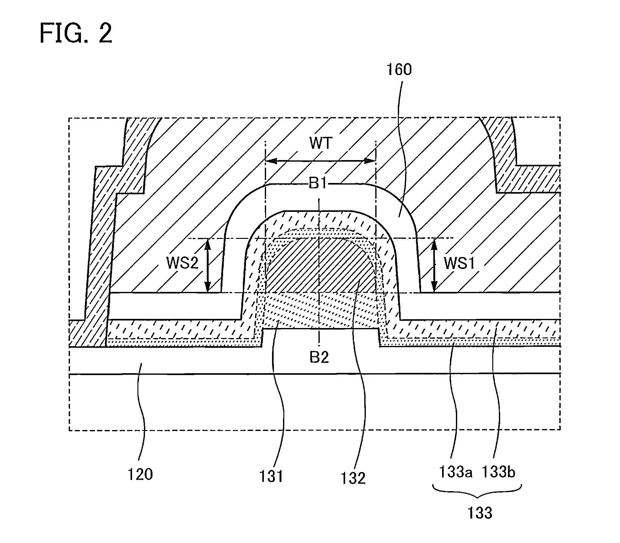
[0050]A transistor 100 illustrated in FIGS. 1A to 1C and FIG. 2 includes a base insulating film 120 formed over a substrate 110; a stack in which a first oxide semiconductor layer 131 and a second oxide semiconductor layer 132 are provided ...
embodiment 2
[0119]In this embodiment, a method for forming the transistor 100, which is described in Embodiment 1 with reference to FIGS. 1A to 1C, is described with reference to FIGS. 7A to 7C and FIGS. 8A to 8C.
[0120]For the substrate 110, a glass substrate, a ceramic substrate, a quartz substrate, a sapphire substrate, or the like can be used. Alternatively, a single crystal semiconductor substrate or a polycrystalline semiconductor substrate made of silicon, silicon carbide, or the like, a compound semiconductor substrate made of silicon germanium or the like, a silicon-on-insulator (SOI) substrate, or the like can be used. Further alternatively, any of these substrates further provided with a semiconductor element can be used.
[0121]The base insulating film 120 can be formed by a plasma CVD method, a sputtering method, or the like using an oxide insulating film of aluminum oxide, magnesium oxide, silicon oxide, silicon oxynitride, gallium oxide, germanium oxide, yttrium oxide, zirconium oxi...
embodiment 3
[0185]In this embodiment, an example of a semiconductor device (storage device) which includes the transistor of one embodiment of the present invention, which can retain stored data even when not powered, and which has an unlimited number of write cycles is described with reference to drawings.
[0186]FIG. 9A is a cross-sectional view of the semiconductor device, and FIG. 9B is a circuit diagram of the semiconductor device.
[0187]The semiconductor device illustrated in FIGS. 9A and 9B includes a transistor3200 including a first semiconductor material in a lower portion, and a transistor 3300 including a second semiconductor material and a capacitor 3400 in an upper portion. Note that the transistor 100 described in Embodiment 1 can be used as the transistor 3300.
[0188]One electrode of the capacitor 3400 is formed using the same material as a source electrode layer or a drain electrode layer of the transistor 3300, the other electrode of the capacitor 3400 is formed using the same mate...
PUM
 Abstract
Description
Claims
Application Information