Integrated circuit for communication

a technology of integrated circuits and communication circuits, applied in the direction of transmission, electrical equipment, etc., can solve the problems of design, assembling and/or manufacturing efforts of wireless devices, incurring extra costs, and adding to the overall cost, so as to achieve convenient deployment, effective cost reduction, and compact pcb

Active Publication Date: 2016-03-08
MEDIATEK SINGAPORE PTE LTD SINGAPORE
View PDF20 Cites 4 Cited by
  • Summary
  • Abstract
  • Description
  • Claims
  • Application Information

AI Technical Summary

Benefits of technology

[0013]To address issues of prior arts, the present invention provides an integrated circuit which achieves easy deployment, effective cost reduction, compact PCB area and OOB blocking compliance with fully embedded (on-chip) impedance matching circuitry and single-end to differential conversion circuitry.
[0018]The main amplifier is electrically coupled between the internal port and a high-frequency port, and is capable of amplifying a first signal at the internal port and accordingly providing a second signal at the high-frequency port. According to detection of the blocker detector, when blocker is not detected, the main amplifier is capable of operating in a normal mode to amplify the first signal by a first gain; on the other hand, when blocker is detected, the main amplifier is capable of operating in an OOB mode to amplify the first signal by a second gain which differs from the first gain. In an embodiment, the first gain for the normal mode is greater than the second gain for the OOB mode; i.e., the main amplifier drops gain during the OOB mode to prevent weak wanted in-band signal from being desensitized by strong OOB blockers.
[0019]The mixer circuit is electrically coupled between the high-frequency port and a low-frequency port, capable of mixing the second signal with the oscillation signal, i.e., local oscillation signal. In an embodiment, the mixer circuit includes a main mixer and an auxiliary mixer. In response to detected result of the blocker detector, when blocker is not detected, the mixer circuit is capable of operating in a normal mode to enable the main mixer and disable the auxiliary mixer; on the other hand, when blocker is detected, the mixer circuit is capable of operating in an OOB mode to enable both the main mixer and the auxiliary mixer. When both the main mixer and the auxiliary mixer are enabled, the mixer circuit can exploit more driving current and power to enhance performance of mixing, e.g., to achieve higher linearity and lower phase noise. In an embodiment, the auxiliary mixer is a duplicate of the main mixer.

Problems solved by technology

Hence, how to reduce design, assembling and / or manufacturing effort and cost of wireless device, as well as how to enhance performance of wireless device, have become key challenges for modern electrical engineering.
Although off-chip SAW filter(s) or BALUN(s) may contribute to suppression of blockers, both incur extra costs.
Furthermore, to implement the external SAW filter and / or BALUN, extra impedance matching components (networks) are needed, which also add on the overall cost.
Even with fully devoted effort, the resultant PCB placement and routing are sensitive to variations, and lack flexibility and / or reusability to be generally adopted by different types of devices.

Method used


Image

  • Integrated circuit for communication
  • Integrated circuit for communication
  • Integrated circuit for communication

Examples


Embodiment Construction

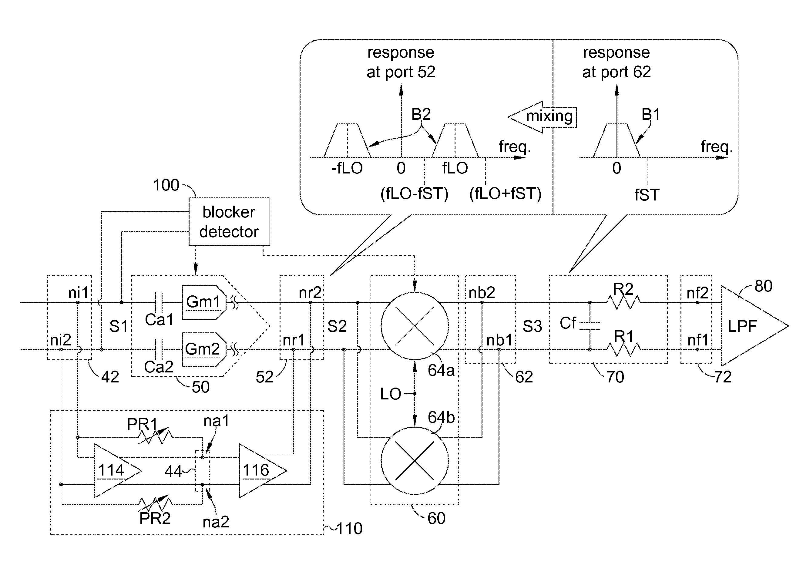
[0033]Please refer to FIG. 4 illustrating an IC 30 according to an embodiment of the invention. The IC 30 can be a packaged die for RF wireless communication; for wireless signal receiving, the IC 30 includes a receiver circuit 120 with two terminals (pins) RXI and GND. The receiver circuit 120 includes an embedded resonator 40, an amplifier 50 (e.g., a current mode LNA), a mixer circuit 60, a translation filter 70, a low-pass filter (LPF) 80 and an analog to digital converter (ADC) 90, along with a blocker detector 100 and an embedded matching circuit 110.

[0034]The terminal GND is electrically coupled to a supply voltage VSS (e.g., a ground voltage). The terminal RXI (receiver terminal) is capable of receiving a single-end RF signal S0 from an antenna (not shown). For example, the terminal RXI can be a low-band receiver terminal for receiving a low-band signal S0 at about 850 MHz, and the receiver circuit 120 can therefore be a low-band receiver circuit configured for low-band rece...


PUM


Abstract

The present invention provides an integrated circuit for communication, e.g., for mobile radio-frequency (RF) telecommunication, including a resonator, a main amplifier, a matching circuit, a blocker detector, a mixer circuit, and a translation filter. The resonator provides conversion from single-end to differential, and filtering function for rejecting blockers at harmonics of local oscillation signal. The blocker detector detects occurrence of blocker; according to whether blocker exists, the main amplifier amplifies differential signal of the resonator by different gains, and the mixer circuit mixes amplified signal with different numbers of mixers. The translation filter contributes to rejection of blockers closed to in-band by providing a first pass band which is translated to a second pass band by the mixer circuit. The matching circuit provides impedance match.

Description

[0001]This application claims the benefit of U.S. provisional application No. 61 / 868,673, filed Aug. 22, 2013, the subject matter of which is incorporated herein by reference.FIELD OF THE INVENTION[0002]The present invention relates to integrated circuit (IC) for communication, and more particularly, to IC which can properly function with minimum external support circuitry to reduce overall cost, and can effectively suppressing interfering blockers.BACKGROUND OF THE INVENTION[0003]Wireless communication, e.g., mobile radio-frequency (RF) telecommunication, positioning and / or networking, has becomes an essential portion of contemporary information society. Wireless communication is implemented by associated wireless device, e.g., mobile phone, cellular phone or portable computer, compliant to specification (standards and / or protocols) of the wireless communication. Hence, how to reduce design, assembling and / or manufacturing effort and cost of wireless device, as well as how to enhan...

Claims


Application Information

Patent Timeline
Patent Type & Authority Patents(United States)
IPC IPC(8): H04B1/10
CPCH04B1/109H04B1/1027H04B1/1036
Inventor ONG, BENG-HWEEKHOO, EE-SZESHANA'A, OSAMA K A
Owner MEDIATEK SINGAPORE PTE LTD SINGAPORE
Why Eureka
Try Eureka