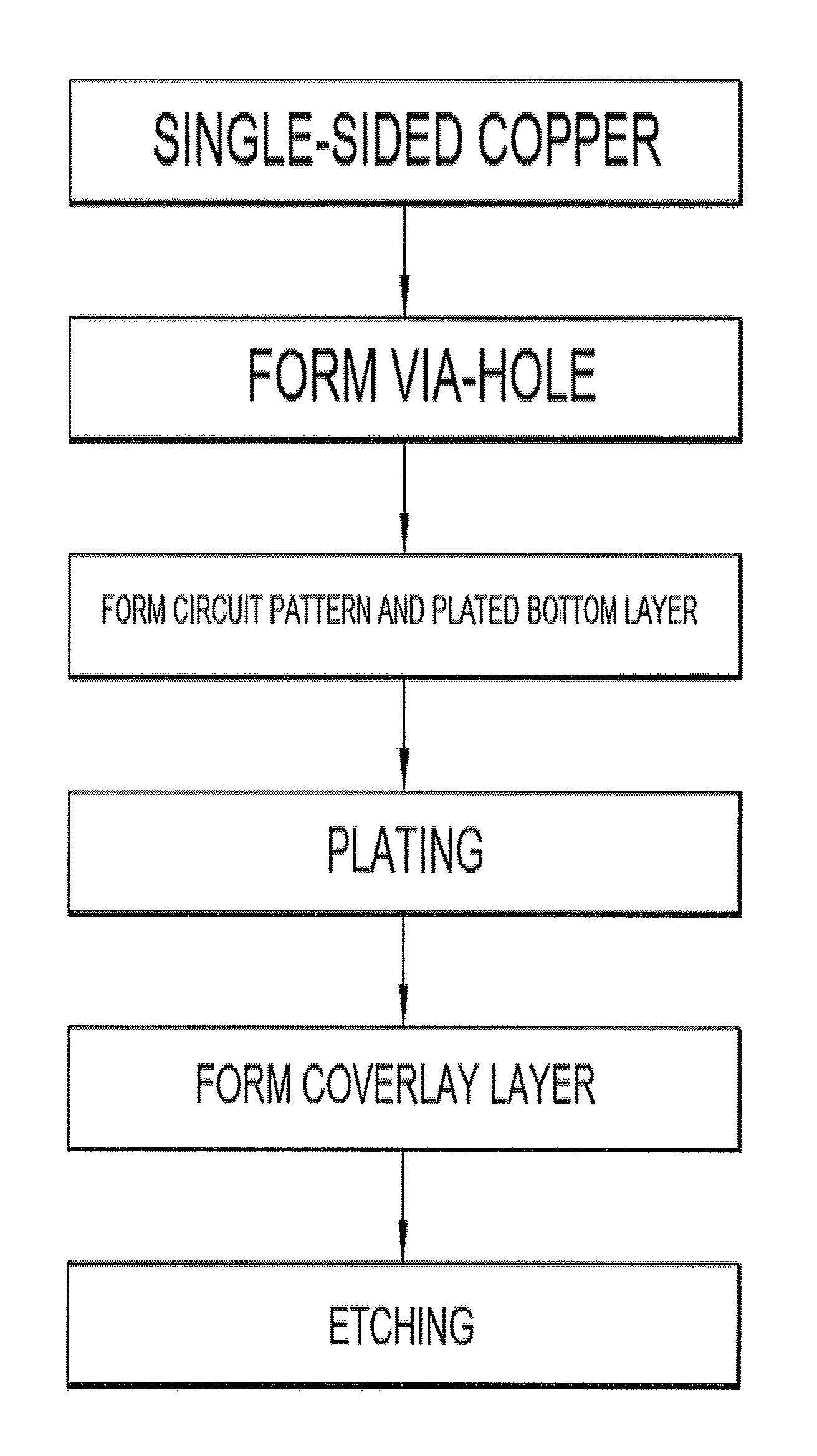
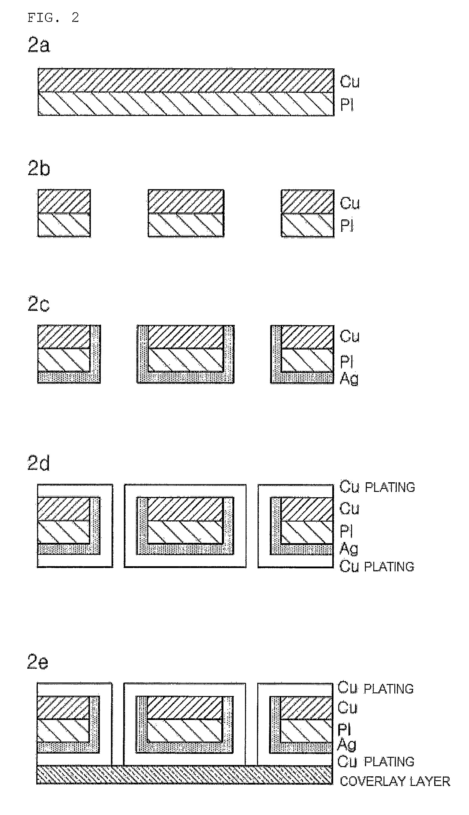
Method for manufacturing a double-sided printed circuit board
a printed circuit board and double-sided technology, applied in the direction of printed element electric connection formation conductive pattern reinforcement, etc., can solve the problems of complex manufacturing process complex structure of wiring, etc., to achieve precise and highly conductive circuit pattern, high reliability, and reduce raw materials and manufacturing processes
- Summary
- Abstract
- Description
- Claims
- Application Information
AI Technical Summary
Benefits of technology
Problems solved by technology
Method used
Image

Examples
example 2
[0104]A double-sided printed circuit board was manufactured by the same method as in Example 1 except that a conductive paste was prepared as follow in a step of forming a circuit pattern using the conductive paste and filling the conductive paste to form a plated bottom layer.
[0105]A reactor with a stirrer was charged with 15.34 g of isopropyl ammonium isopropylcarbamate (81.1 mM), 49.07 g of 2-ethylhexyl ammonium 2-ethylhexylcarbamate (162.2 mM), and 18.8 g of silver oxide (81.1 mM) and stirred for 3 hours, and then this reactant was filtered using a mesh filter to remove unreacted silver oxide, thereby preparing a conductive silver paste having a silver solid content of 21%.
example 3
[0106]A double-sided printed circuit board was manufactured by the same method as in Example 1 except that a conductive paste was prepared as follow in a step of forming a circuit pattern using the conductive paste and filling the conductive paste to form a plated bottom layer.
[0107]A reactor with a stirrer was charged with 812.1 g of 2-ethylhexyl ammonium 2-ethylhexylcarbamate (2.68 M) and 187.9 g of silver oxide (0.89 M) and stirred for 3 hours, thereby preparing a silver complex compound. The reactor with a stirrer was charged with 20.44 g of the prepared silver complex compound, 36.42 g of silver nanoparticles (Ferro Co.), and 43.14 g of 2-ethylhexyl ammonium 2-ethylhexylcarbamate, and primary stirring was performed. Secondary dispersion was performed on the mixture obtained by primary stirring, thereby preparing a conductive silver paste having a silver solid content of 40%.
example 4
[0108]A double-sided printed circuit board was manufactured by the same method as in Example 1 except that a conductive paste was prepared as follow in a step of forming a circuit pattern using the conductive paste and filling the conductive paste to form a plated bottom layer.
[0109]A reactor with a stirrer was charged with 812.1 g of 2-ethylhexyl ammonium 2-ethylhexylcarbamate (2.68 M) and 187.9 g of silver oxide (0.89 M) and stirred for 3 hours, thereby preparing a silver complex compound. The reactor with a stirrer was charged with 25.52 g of the prepared silver complex compound, 45.53 g of silver nanoparticles (Ferro Co.), and 28.95 g of 2-ethylhexyl ammonium 2-ethylhexylcarbamate, and primary stirring was performed. Secondary dispersion was performed on the mixture obtained by primary stirring, thereby preparing a conductive silver paste having a silver solid content of 50%.
PUM
| Property | Measurement | Unit |
|---|---|---|
| thickness | aaaaa | aaaaa |
| size | aaaaa | aaaaa |
| size | aaaaa | aaaaa |
Abstract
Description
Claims
Application Information