Semiconductor device

a technology of semiconductors and encapsulating resins, applied in the direction of coupling device connections, coupling protective earth/shielding arrangements, transistors, etc., can solve the problems of deteriorating product reliability, degrading moisture resistance, and poor adhesion between copper and encapsulating resins

Active Publication Date: 2009-01-20
LAPIS SEMICON CO LTD
View PDF7 Cites 38 Cited by
  • Summary
  • Abstract
  • Description
  • Claims
  • Application Information

AI Technical Summary

Benefits of technology

[0015]In the present invention, the shield section in which the strip metallic thin films are disposed and formed in parallel is provided so as to cover the analog circuit. Thus, since the insulating layer and the encapsulating resin are adhered to each other with the strip metallic thin films interposed therebetween, the peeling between the encapsulating resin and the metallic thin films is avoided as in the shield section having a wide area. Accordingly, advantageous effects are brought about in that degradation of moisture resistance can be prevented and the reliability of a product can be enhanced.
[0016]The width of each redistribution wiring and the width of each metallic thin film of the shield section are identical and set to 180 μm or less, and they are manufactured in the same process. Further, the interval between the plural respective strip metallic thin films constituting the shield section is set to 10 μm even at the minimum and set so as not to exceed 50 μm.

Problems solved by technology

Since, however, the adhesion between copper and an encapsulating resin is essentially poor, the adhesion between the shield section 4b and an encapsulating portion such as the second insulating layer 7 that covers the shield section 4b is degraded when the area of the copper plating film of the shield section 4b increases, and failures such as peeling, etc. occur due to the difference in thermal expansion coefficient and the like, thus degrading moisture resistance.
Therefore, a problem arises in that the reliability of a product is deteriorated.

Method used


Image

  • Semiconductor device
  • Semiconductor device
  • Semiconductor device

Examples


first preferred embodiment

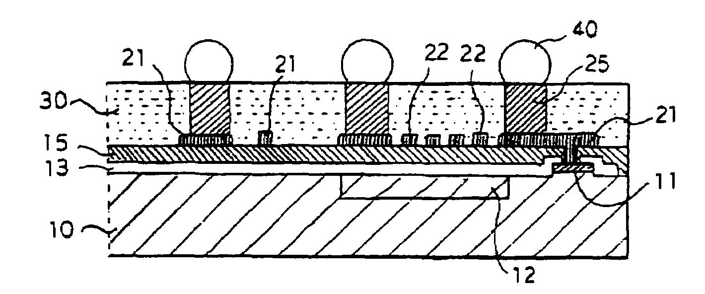
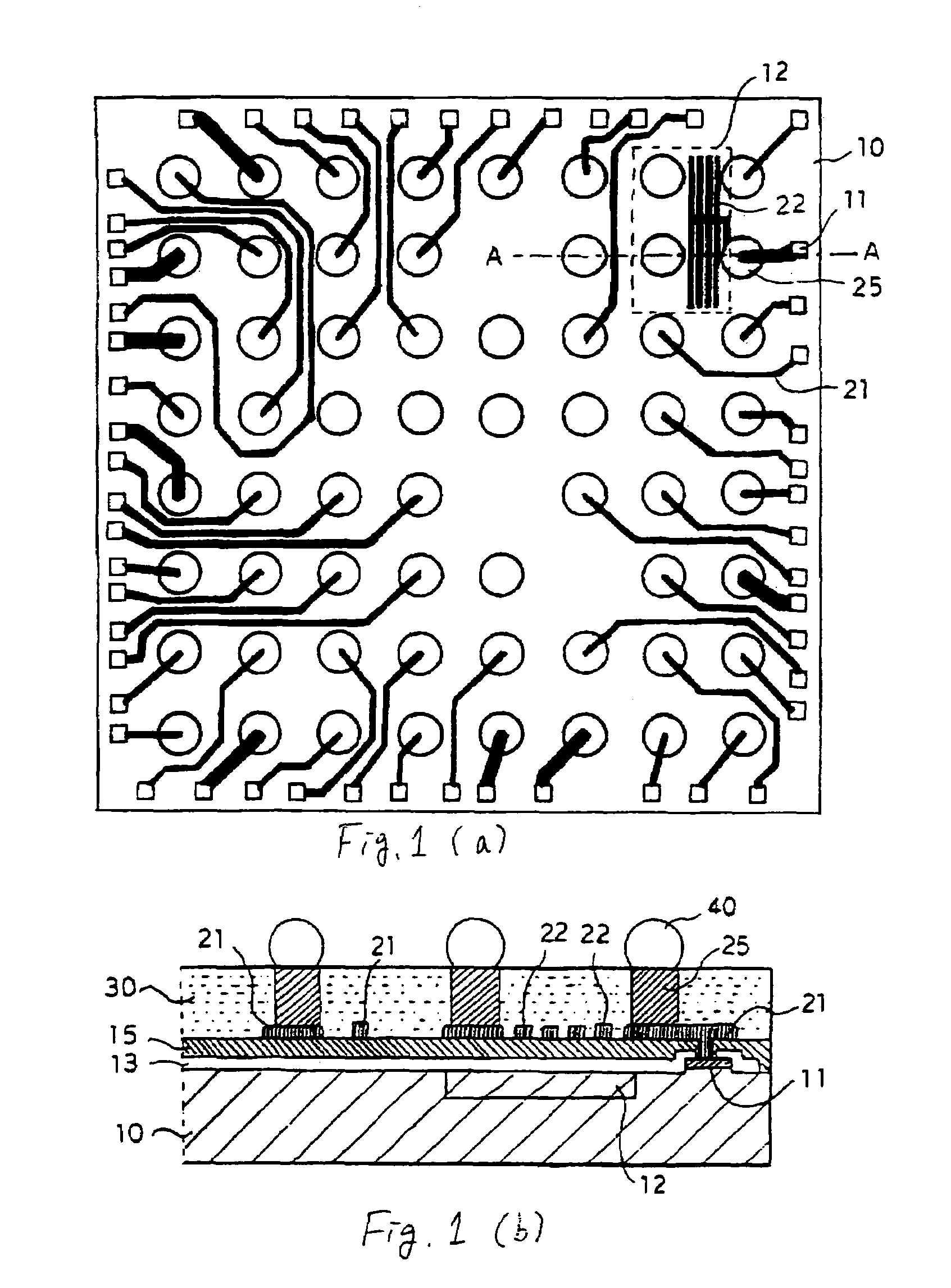
[0022]FIG. 1 is a configurational view of a semiconductor device showing an embodiment of the present invention, wherein FIG. 1(a) is a plan view thereof, and FIG. 1(b) is an enlarged sectional view of a portion taken along line A-A in FIG. 1(a).

[0023]The semiconductor device is one of a CSP type and has a silicon substrate 10 in which a large number of electrode pads 11 are arranged in its outer peripheral portion and circuit elements are formed in an internal circuit forming surface. An analog circuit 12 including, for example, an operational amplifier, an analog / digital converter, a digital / analog converter, a phase-locked loop, etc., and circuit blocks such as a digital circuit, etc. other than ones referred to above are formed in the circuit forming surface. A passivation film 13 comprised of, for example, a silicon nitride film is formed on the surface of the silicon substrate 10. Openings or apertures corresponding to the electrode pads 11 are defined in the passivation film ...


PUM


Abstract

Strip metallic thin films each having a width of 180 μm or so are disposed in parallel at intervals of 10 μm to 50 μm on the surface of a protection layer formed on the silicon substrate and at their corresponding spots located on the upper side of an analog circuit formed in a silicon substrate. These strip metallic thin films are connected to one another at their ends or centers to form a comb-like shield section and one end thereof is connected to its corresponding external connecting post. Incidentally, the shield section is formed by copper plating in the same process as redistribution wirings that connect electrode pads at an outer peripheral portion of the silicon substrate to their corresponding external connecting posts. Since the encapsulating resin and the protection layer are reliably adhered to each other when the upper portions of the redistribution wirings and the shield section are sealed with the encapsulating resin, the shield section is adhered to the encapsulating resin and has no fear of being peeled therefrom.

Description

BACKGROUND OF THE INVENTION[0001]The present invention relates to a semiconductor device of a CSP (Chip Size Package) type, and particularly to a structure of a redistribution wiring layer for the semiconductor device.[0002]FIG. 2 is a configurational view of a conventional semiconductor device described in, for example, one (Japanese Unexamined Patent Publication No. 2004-31790) of patent documents 1, 2 and 3 (Japanese Unexamined Patent Publication Nos. 2004-31790, 2004-214561 and 2003-243570), wherein FIG. 2(a) is a plan view thereof, and FIG. 2(b) is a sectional view of a portion taken along line X-X in FIG. 2(a).[0003]The present semiconductor device is of a CSP type and includes respective circuit blocks for a power supply circuit 51, an operational amplifier 52, a comparison amplifier 53, an analog circuit of an RF transmit-receive section 54 and a digital circuit of a logic section 55 all formed in its circuit forming surface. The semiconductor device has an IC 1 in which a l...

Claims


Application Information

Patent Timeline
Patent Type & Authority Patents(United States)
IPC IPC(8): H01L23/552
CPCH01L23/3114H01L23/528H01L23/552H01L2224/16235H01L2924/01078H01L2924/3025H01L2224/16H01L2224/05024H01L2224/05008H01L2224/05022H01L2224/05001H01L2224/05147H01L2224/05647H01L24/05H01L2224/02377H01L2224/0616H01L24/02H01L2924/00014
Inventor SHIRAISHI, YASUSHI
Owner LAPIS SEMICON CO LTD
Why Eureka
Try Eureka