Method of manufacturing flat-panel display device, apparatus for manufacturing flat-panel display device, and flat-panel display device

a technology for flat-panel display devices and manufacturing methods, applied in the manufacture of electrode systems, electric discharge tubes/lamps, casings of electrical apparatus, etc., can solve the problems of reducing sealing strength, reducing product reliability, and unable to ensure sufficient strength, so as to improve product reliability and simplify manufacturing process

Inactive Publication Date: 2010-03-25
KK TOSHIBA
View PDF0 Cites 37 Cited by
  • Summary
  • Abstract
  • Description
  • Claims
  • Application Information

AI Technical Summary

Benefits of technology

[0008]An object of the present invention is to provide a method of manufacturing a flat-panel display device, an apparatus for manufacturing a flat-panel display device, and a flat-panel display device, capable of achieving an improvement in product reliability and a simplification of a manufacturing process.

Problems solved by technology

However, the above-mentioned methods adopt a structure in which the space exists between the sealing substrate and the light-emitting element, or a structure in which the sealing substrate and the element substrate are joined together only by the frit material, thereby failing to ensure sufficient strength.
For this reason, the damage by the shock occasionally occurs, and hence flat-panel display devices thus configured have only low product reliability.
Moreover, the frit material, before sealing, can possibly be contaminated by the resin or the film, and this surface contamination of the frit reduces sealing strength, which also results in low product reliability.
Furthermore, the need for a reinforcement process to be performed around the periphery of the frit material makes a manufacturing process complicated.

Method used


Image

  • Method of manufacturing flat-panel display device, apparatus for manufacturing flat-panel display device, and flat-panel display device
  • Method of manufacturing flat-panel display device, apparatus for manufacturing flat-panel display device, and flat-panel display device
  • Method of manufacturing flat-panel display device, apparatus for manufacturing flat-panel display device, and flat-panel display device

Examples


first embodiment

[0034]A first embodiment of the present invention will be described with reference to FIGS. 1 to 12.

(A Method of Manufacturing a Flat-Panel Display Device)

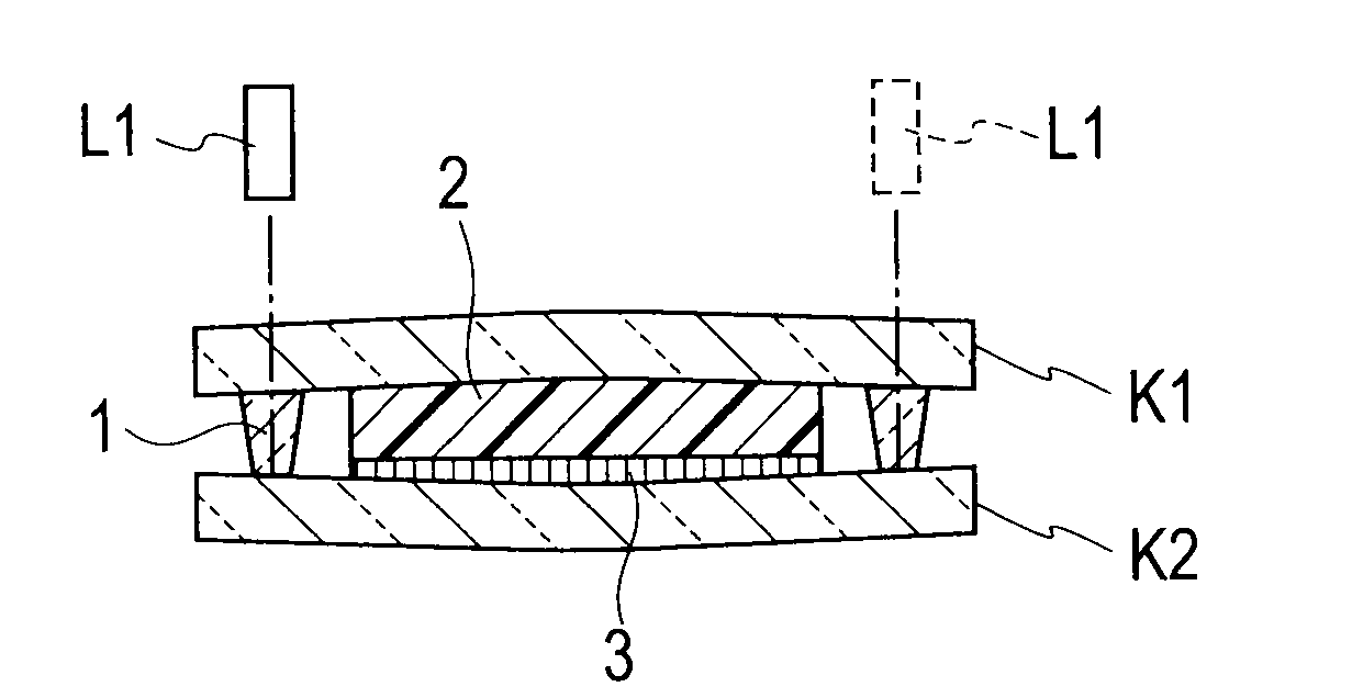
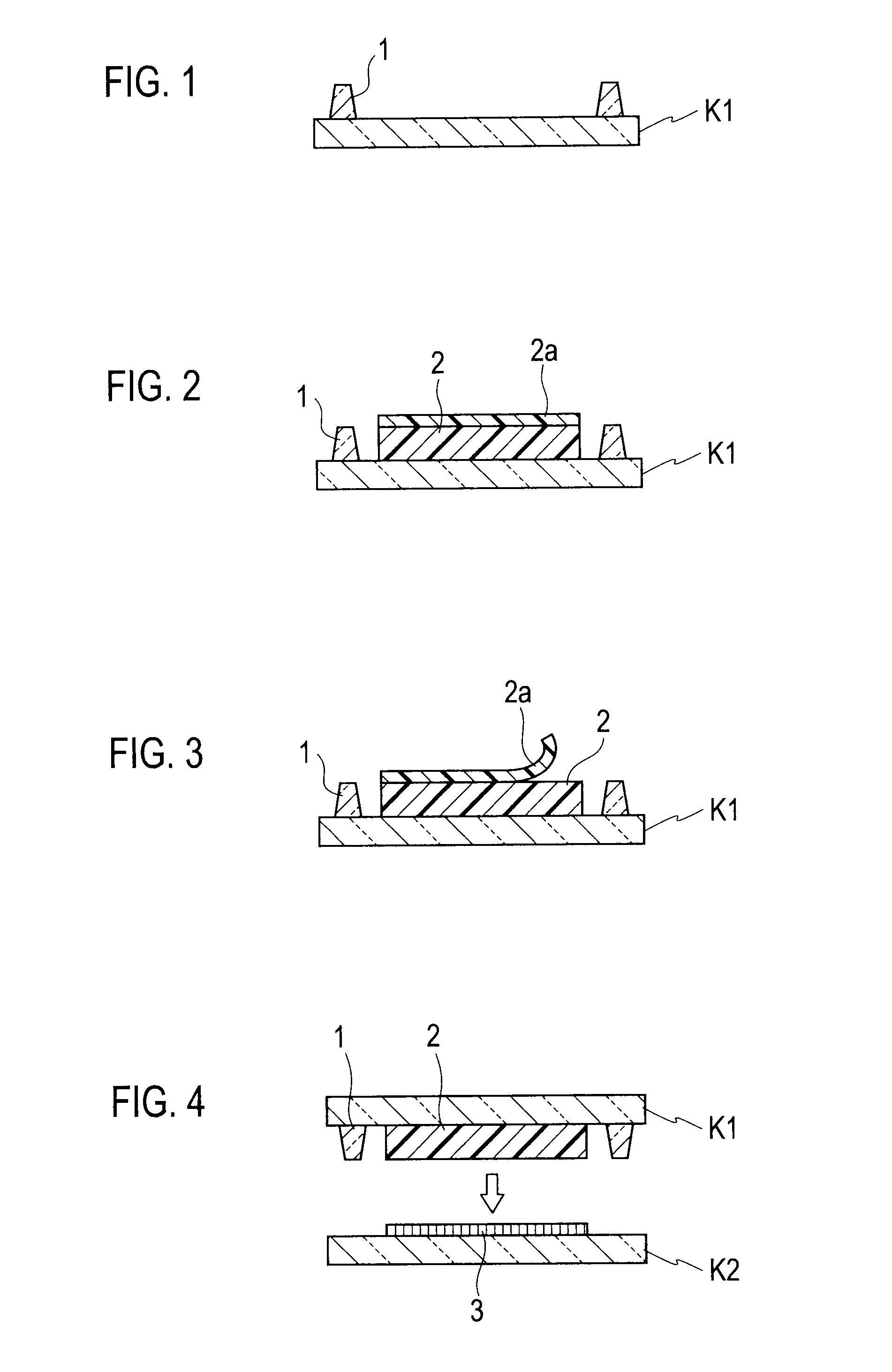
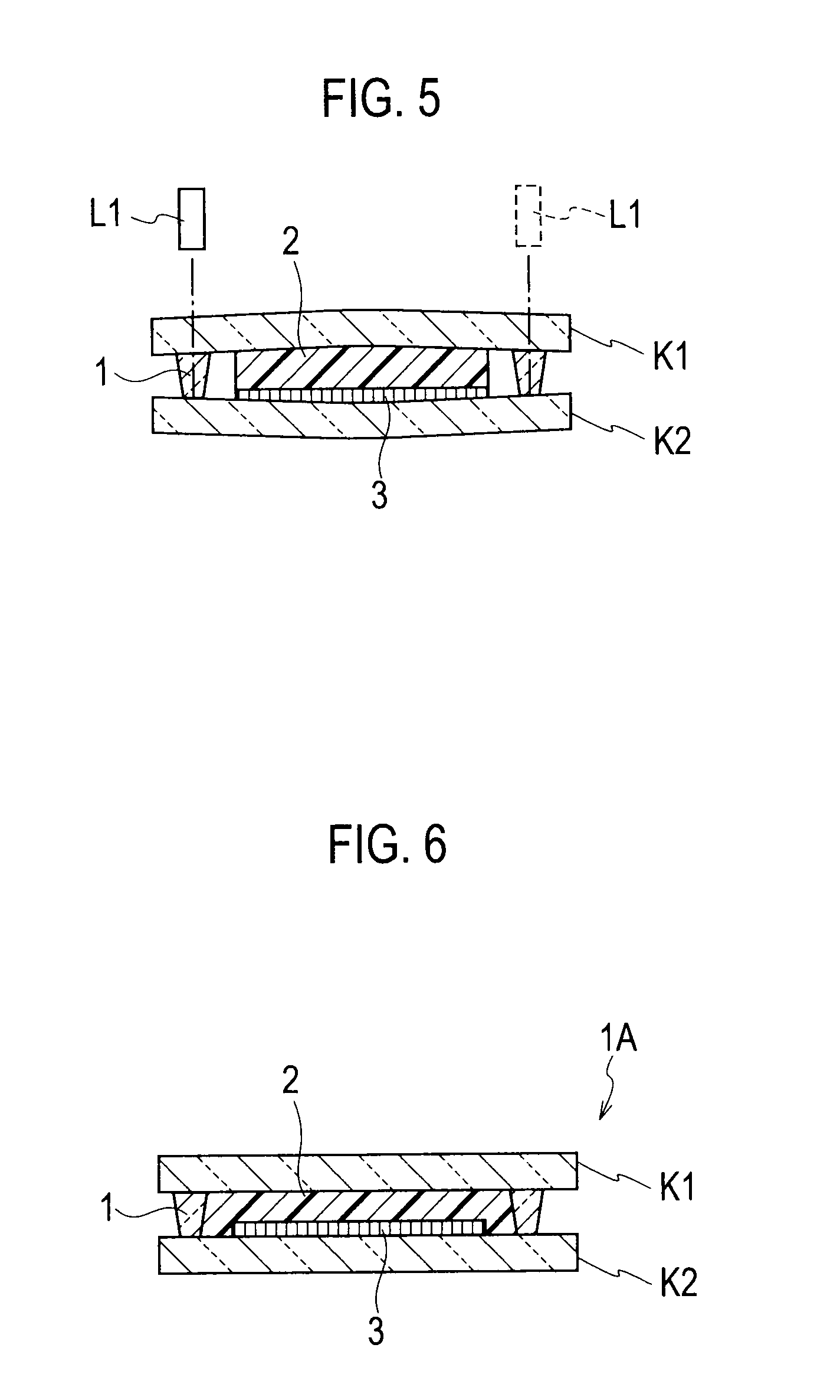
[0035]A process for manufacturing the flat-panel display device according to the first embodiment of the present invention includes a coating and baking process for performing coating and baking of a frit material 1 in the shape of a frame on a sealing substrate K1, as shown in FIG. 1; a film laminating process for mounting and laminating a thermosetting resin film 2 having a protective sheet 2a, both on the sealing substrate K1 and inside the frame-shaped frit material 1, as shown in FIG. 2; a sheet delaminating process for delaminating the protective sheet 2a on the thermosetting resin film 2, as shown in FIG. 3; a lamination process for laminating the sealing substrate K1 having the thermosetting resin film 2 laminated thereon, to an element substrate K2 having plural light-emitting elements 3, as shown in FIG. 4; a frit bondin...

second embodiment

[0073]A second embodiment of the present invention will be described with reference to FIGS. 13 to 17.

[0074]The second embodiment of the present invention is basically the same as the first embodiment. For the second embodiment, therefore, description will be given with regard to different parts from the first embodiment. Incidentally, in the second embodiment, description of the same parts as described for the first embodiment will be omitted.

[0075]A process for manufacturing a flat-panel display device according to the second embodiment of the present invention includes, after the sheet delaminating process shown in FIG. 3 according to the first embodiment, a coating process for coating a sealant 4a in the shape of a frame both on the sealing substrate K1 after delamination of the protective sheet 2a and outside the frame-shaped frit material 1, as shown in FIG. 13; a lamination process for laminating the sealing substrate K1 coated with the sealant 4a to the element substrate K2,...

third embodiment

[0082]A third embodiment of the present invention will be described with reference to FIGS. 18 to 22.

[0083]The third embodiment of the present invention is basically the same as the second embodiment. For the third embodiment, therefore, description will be given with regard to different parts from the second embodiment. Incidentally, in the third embodiment, description of the same parts as described for the second embodiment will be omitted.

[0084]As shown in FIG. 18, the sealing substrate K1 having a frame-shaped sealant 4b mounted thereon is turned upside down so that the thermosetting resin film 2 on the sealing substrate K1 faces the light-emitting elements 3 on the element substrate K2, and the sealing substrate K1 is mounted and laminated on the element substrate K2. The sealant 4b is a thermosetting resin film. The sealant 4b is mounted in the shape of the frame both on the sealing substrate K1 and outside the frame-shaped frit material 1, as is the case with the mounting of...


PUM


Abstract

Disclosed is a method of manufacturing a flat-panel display device, includes: laminating a thermosetting resin film on a sealing substrate; stacking the sealing substrate having the thermosetting resin film laminated thereon, and an element substrate having a light-emitting element together under a vacuum atmosphere with the thermosetting resin film and the light-emitting element facing inwardly, and with a frame-shaped sealing material around the thermosetting resin film interposed between the two substrates; joining the sealing substrate and the element substrate together under a vacuum atmosphere by the sealing material situated between the sealing substrate and the element substrate stacked together; and heat-curing the thermosetting resin film situated between the sealing substrate and the element substrate stacked together, under an air atmosphere.

Description

CROSS REFERENCE OF THE RELATED APPLICATION[0001]This application is based on and claims the benefit of priority from Japanese Patent Application No. 2008-243878, filed on Sep. 24, 2008; the entire contents of which are incorporated herein by reference.BACKGROUND OF THE INVENTION[0002]1. Field of the Invention[0003]The present invention relates to a method of manufacturing a flat-panel display device, an apparatus for manufacturing a flat-panel display device, and a flat-panel display device.[0004]2. Description of the Related Art[0005]A flat-panel display device is used in various kinds of equipment such as a computer's display and a mobile terminal. An organic EL (electroluminescence) display device, for example, has been developed as one type of flat-panel display device. The organic EL display device is the display device capable of having a thinner body than a liquid crystal display device, a plasma display device, or the like and capable of spontaneous light emission as is the ...

Claims


Application Information

Patent Timeline
Patent Type & Authority Applications(United States)
IPC IPC(8): H01J9/20H01J9/38H05K5/00
CPCH01L51/56H01L51/5237H10K50/8426H10K71/00
Inventor MATSUI, TOMOHIROFURUYA, MASAAKI
Owner KK TOSHIBA
Why Eureka
Try Eureka