Wafer level semiconductor package with build-up layer and method for fabricating the same

a technology of build-up layer and semiconductor package, which is applied in the direction of semiconductor device details, semiconductor/solid-state device devices, electrical devices, etc., can solve the problems of limited number of bond pads provided on the chip, warpage can occur during temperature cycling, and limited active surface area, so as to improve the reliability of the effect of the effect of bonding

Active Publication Date: 2005-09-15
SILICONWARE PRECISION IND CO LTD
View PDF5 Cites 39 Cited by
  • Summary
  • Abstract
  • Description
  • Claims
  • Application Information

AI Technical Summary

Benefits of technology

[0010] An objective of the present invention is to provide a wafer level semiconductor package with a build-up layer, which is free from warpage, crack, and delamination problems and enhances the reliability thereof.

Problems solved by technology

However, the number of the bond pads provided on the chip is limited by an area of the active surface and pitches between the bond pads.
However, it is still restricted by the limited area of the active surface of the chip.
Thus, warpage can be resulted during temperature cycling in subsequent processes.
Further, a crack may be occurred in a position of a numeral 624 due to concentration of stresses.
Therefore, a so-called ‘popcorn phenomenon’ would be resulted to thereby not enhancing the reliability of the products.

Method used


Image

  • Wafer level semiconductor package with build-up layer and method for fabricating the same
  • Wafer level semiconductor package with build-up layer and method for fabricating the same
  • Wafer level semiconductor package with build-up layer and method for fabricating the same

Examples


first embodiment

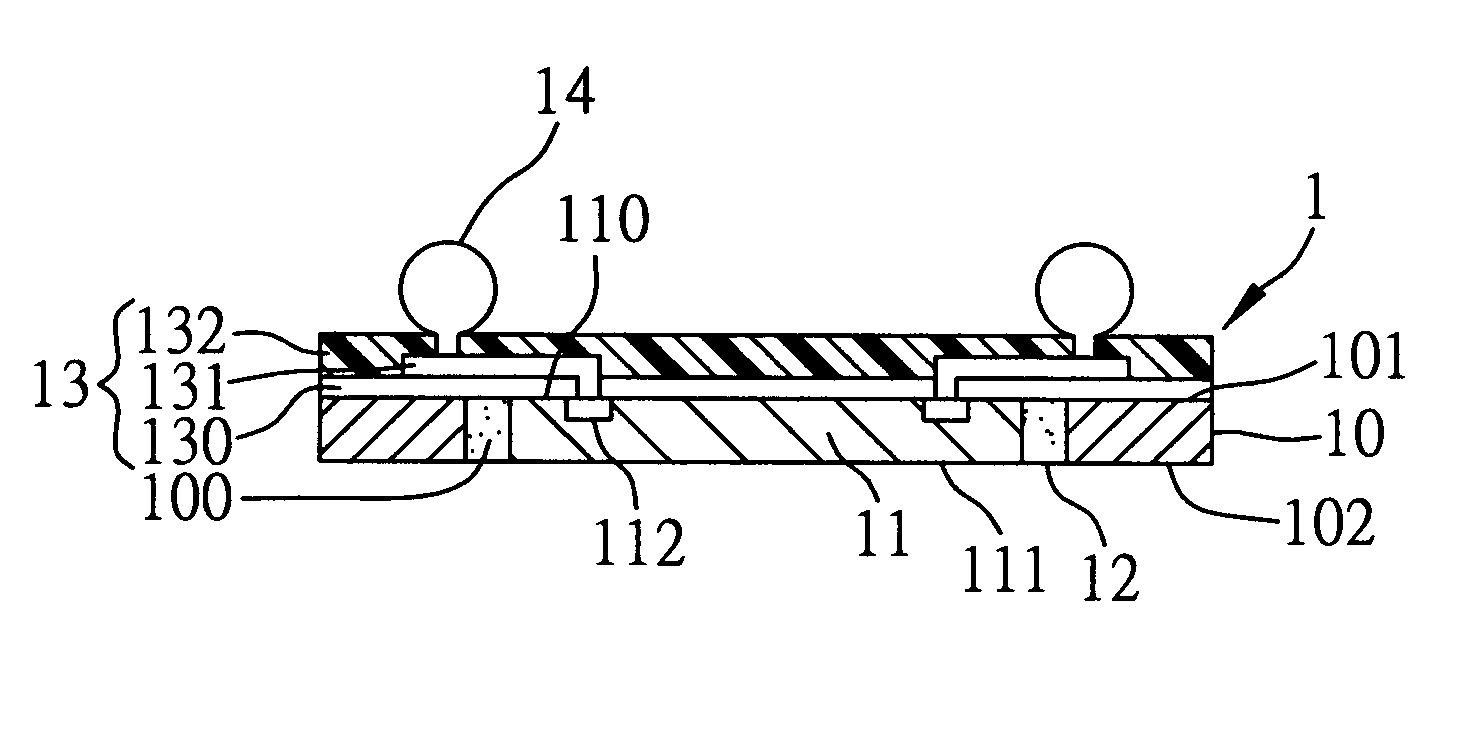
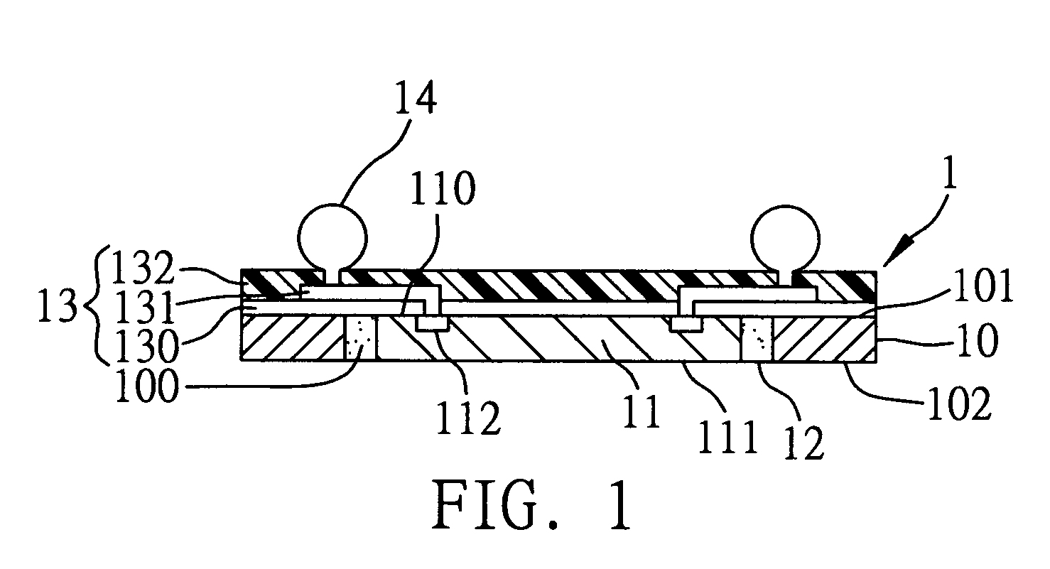
[0029] Referring to FIG. 1, a wafer level semiconductor package with a build-up layer 1 mainly comprises a rigid frame 10 having a through hole 100, a chip 11 received in the through hole 100 of the rigid frame 10, a low-modulus buffer material 12 filled between the rigid frame 10 and the chip 11, a build-up layer 13 disposed on the rigid frame 10 and the chip 11 and a plurality of solder balls 14 (equivalent to the foregoing conductive elements) mounted on the build-up layer 13.

[0030] The rigid frame 10 is made of a material selected from the group consisting of glass, metal (such as copper metal and the like) and thermosetting materials (such as polyimide resins, bismaleimide triazine resins (BT resins), RF-4, and the like). The rigid frame 10 can serve as a primary structured body for the wafer level semiconductor package 1 without causing a warpage problem as it does not generate warpage under high temperature or during temperature cycling of fabrication. Furthermore, unlike th...

second embodiment

[0044] The fabrication to be demonstrated in the second embodiment of the present invention is similar to that of the foregoing first embodiment. Thus, only differences between these two embodiments are further described by using the drawings.

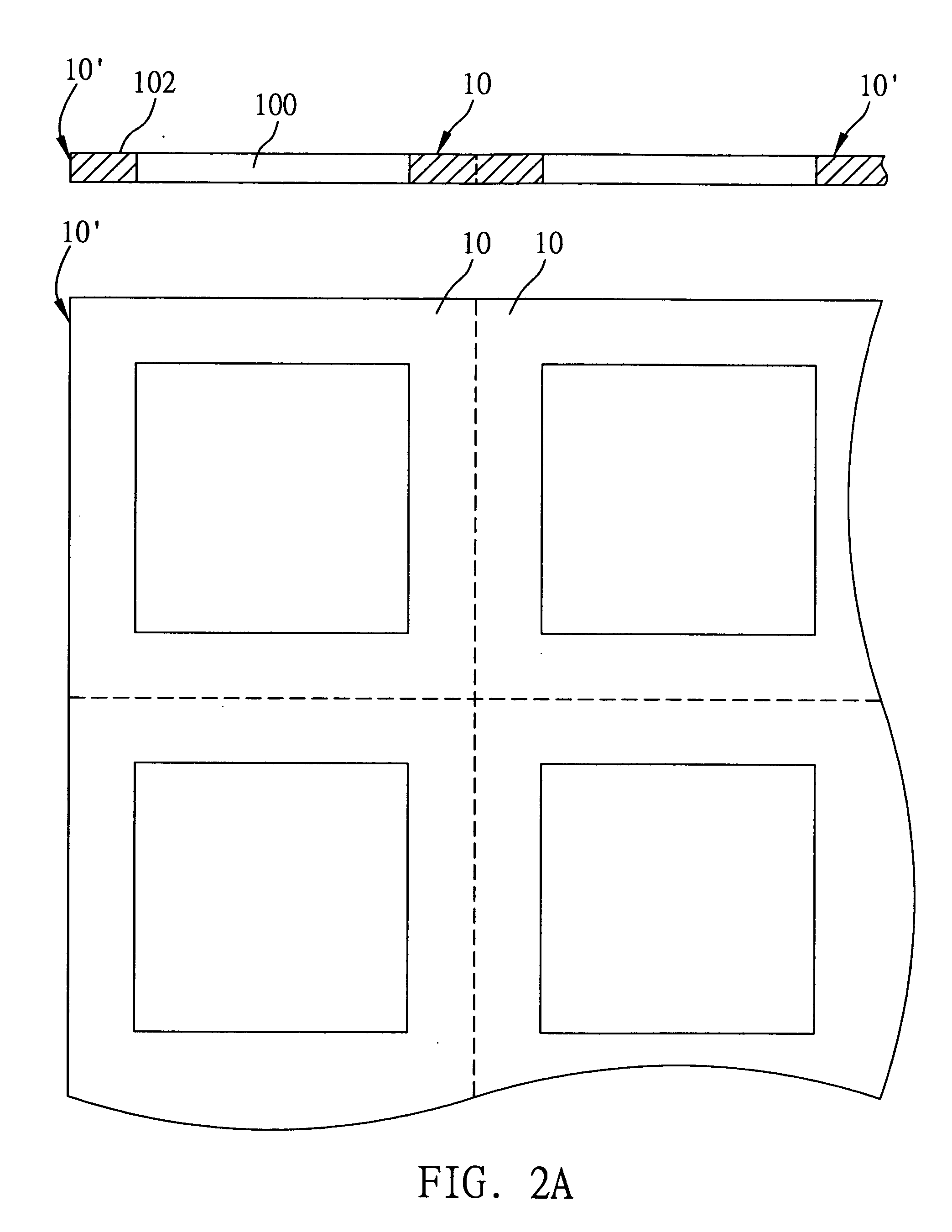
[0045] Referring to FIG. 3A, a module board 20′ consisting of a plurality of rigid frames 20 arranged in arrays is provided, in which each of the rigid frames 20 comprises a rectangular through hole 200, a first surface 201 and a relative second surface 202. Also, a jig 26 having a receiver 260 is provided, in which a film 27 is adhered on bottom of the receiver 260 and a plurality of chips 21 is mounted on predetermined positions on the film 27. Materials of the film 27 are selected from those providing an adhesion between the film 27 and the jig 26 larger than that between the film 27 and the chip 21 and between the film 27 and the module board 20′.

[0046] Referring to FIG. 3B, the module board 20′ is placed into the receiver 260 of the jig ...

third embodiment

[0050]FIG. 4 is a cross-sectional view of a wafer level semiconductor package according to the third embodiment of the present invention. The structure of a wafer level semiconductor package 3 according to the third embodiment is similar to that of the first embodiment. Differently, a thickness of a chip 31 is smaller than that of a rigid frame 30. Thus, when a low-modulus buffer material 32 is filled into a space between the chip 31 and the rigid frame 30 using a screen-printing method, an inactive surface 311 of the chip 31 is covered by the low-modulus buffer material 32, such that the chip 31 is completely encapsulated by the low-modulus buffer material 32 except for an active surface 310 of the chip 31. Therefore, criteria required for a consistent thickness for the rigid frame 30 and the chip 31 can be less stringent, so that when the thickness of the chip 31 is smaller than that of the rigid frame 30, a thickness difference is between 0.05 mm and 0.5 mm, and preferably 0.1 mm...


PUM


Abstract

A wafer level semiconductor package with a build-up layer is provided, which includes a glass frame having a through hole for receiving a semiconductor chip therein, a low-modulus buffer material filled within the space formed between the semiconductor chip and the glass frame, a build-up layer formed on the glass frame and the semiconductor chip such that the build-up layer is electrically connected to the semiconductor chip, and a plurality of conductive elements mounted on the build-up layer so that the semiconductor chip is electrically connected to external devices. With the use of the glass frame and low-modulus buffer material, the wafer level semiconductor package thus-obtained is free from warpage, chip-crack, and delamination problems and the reliability thereof is enhanced. A method for fabricating the wafer level semiconductor package is also provided.

Description

FIELD OF THE INVENTION [0001] The present invention relates to a wafer level semiconductor package and a method for fabricating the same, and more particularly, to a wafer level semiconductor package having a build-up layer formed on an active surface of a chip, by which external contacts for implantation of solder balls expose from the active surface of the chip and a method for fabricating the same. BACKGROUND OF THE INVENTION [0002] Along with requirements of tiny and light electronic products, semiconductor packages serving as central components for the electronic products are gradually becoming miniaturized. Chip scale package (CSP) which is one sort of miniaturized semiconductor packages is characterized that the size of such package is equivalent to or about 1.2 times bigger than that of the chip. [0003] Furthermore, in addition to miniaturization for the semiconductor packages, high integration and the number of input / output connections (I / O connections) for electrically con...

Claims


Application Information

Patent Timeline
Patent Type & Authority Applications(United States)
IPC IPC(8): H01L21/44
CPCH01L21/6835H01L2224/12105H01L2224/04105H01L2224/19H01L2224/20H01L2224/97H01L2924/01029H01L2924/15311H01L2924/18162H01L24/97H01L2224/0401H01L2224/73267H01L2224/32245H01L2924/01033H01L24/19H01L21/568H01L24/96H01L2224/32225H01L2224/82H01L2924/351H01L2924/181H01L2924/12042H01L2924/3511H01L2924/00
Inventor HUANG, CHIEN-PINGHSIAO, CHENG-HSUHUANG, CHIH-MING
Owner SILICONWARE PRECISION IND CO LTD
Why Eureka
Try Eureka