
Display device and method for driving the same

a technology of display device and display device, which is applied in the direction of static indicating device, instruments, etc., can solve the problems of smear on the screen, delay in response time, and difficulty in correctly displaying gray levels

Active Publication Date: 2016-05-03
SAMSUNG DISPLAY CO LTD
View PDF12 Cites 16 Cited by
  • Summary
  • Abstract
  • Description
  • Claims
  • Application Information

AI Technical Summary

Benefits of technology

This patent is about a display device and its driving method that can solve problems such as response time, sticking, and smearing to achieve high-quality and high-definition display. The technical effects of the patent include reducing response time delay, eliminating sticking, compensating for threshold voltage variation, and reducing smearing caused by on-bias voltage application.

Problems solved by technology

However, in the case where the compensation circuit is used to display a target luminance, the response time varies depending on increases or decreases of data voltage due to hysteresis such that it is difficult to correctly display gray levels.
For example, the response time may be delayed when the OLED display is driven to display luminance from black to white, and this problem may cause sticking when a text is scrolled on a screen.
However, a characteristic curve of the first transistor changes when the on-bias voltage is applied, thereby causing smear on the screen when the gray levels are displayed.

Method used


Image

  • Display device and method for driving the same
  • Display device and method for driving the same
  • Display device and method for driving the same

Examples


Embodiment Construction

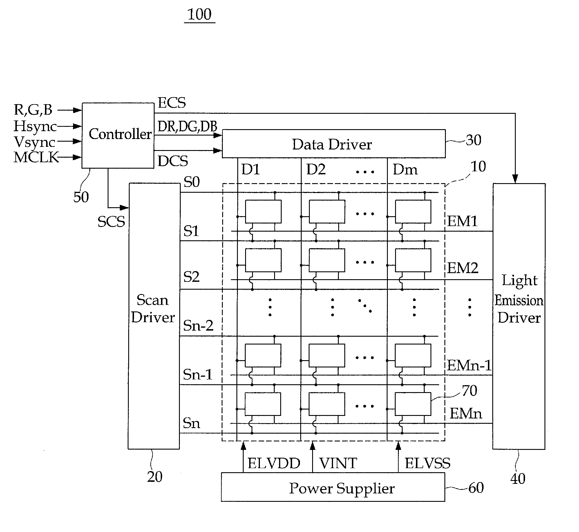
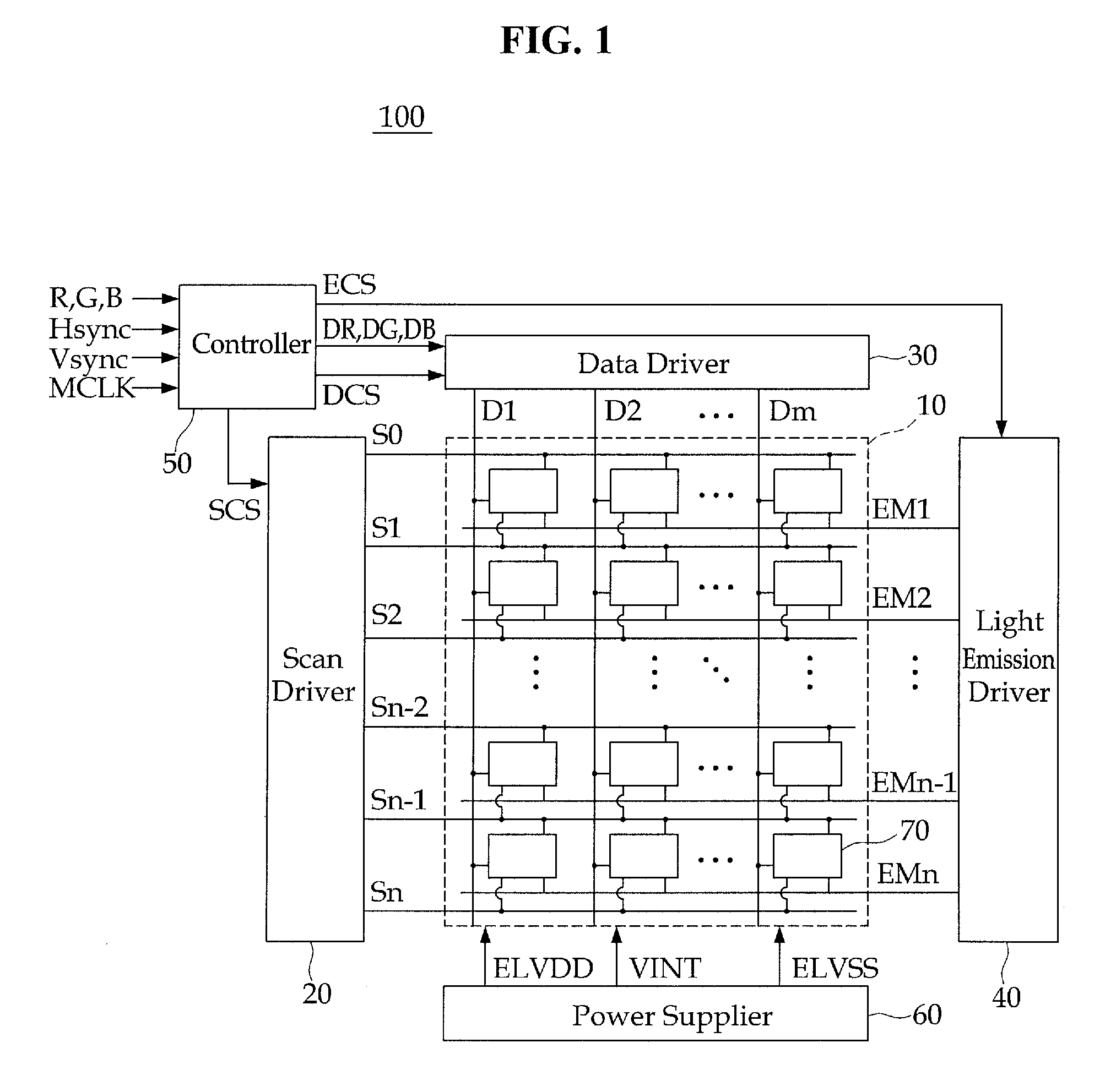
[0036]Aspects and features of the present invention and methods for achieving them will be made clear from embodiments described below in detail with reference to the accompanying drawings. The present invention may, however, be embodied in many different forms and should not be construed as being limited to the embodiments set forth herein. Rather, these embodiments are provided so that this disclosure will be thorough and complete, and will fully convey the scope of the present invention to those skilled in the art. The present invention is merely defined by the scope of the claims, and equivalents thereof. Therefore, well-known constituent elements, operations and techniques are not described in detail in the embodiments in order to prevent the present invention from being obscurely interpreted. Like reference numerals refer to like elements throughout the specification.

[0037]The spatially relative terms “below”, “beneath”, “lower”, “above”, “upper”, and the like, may be used her...


PUM


Abstract

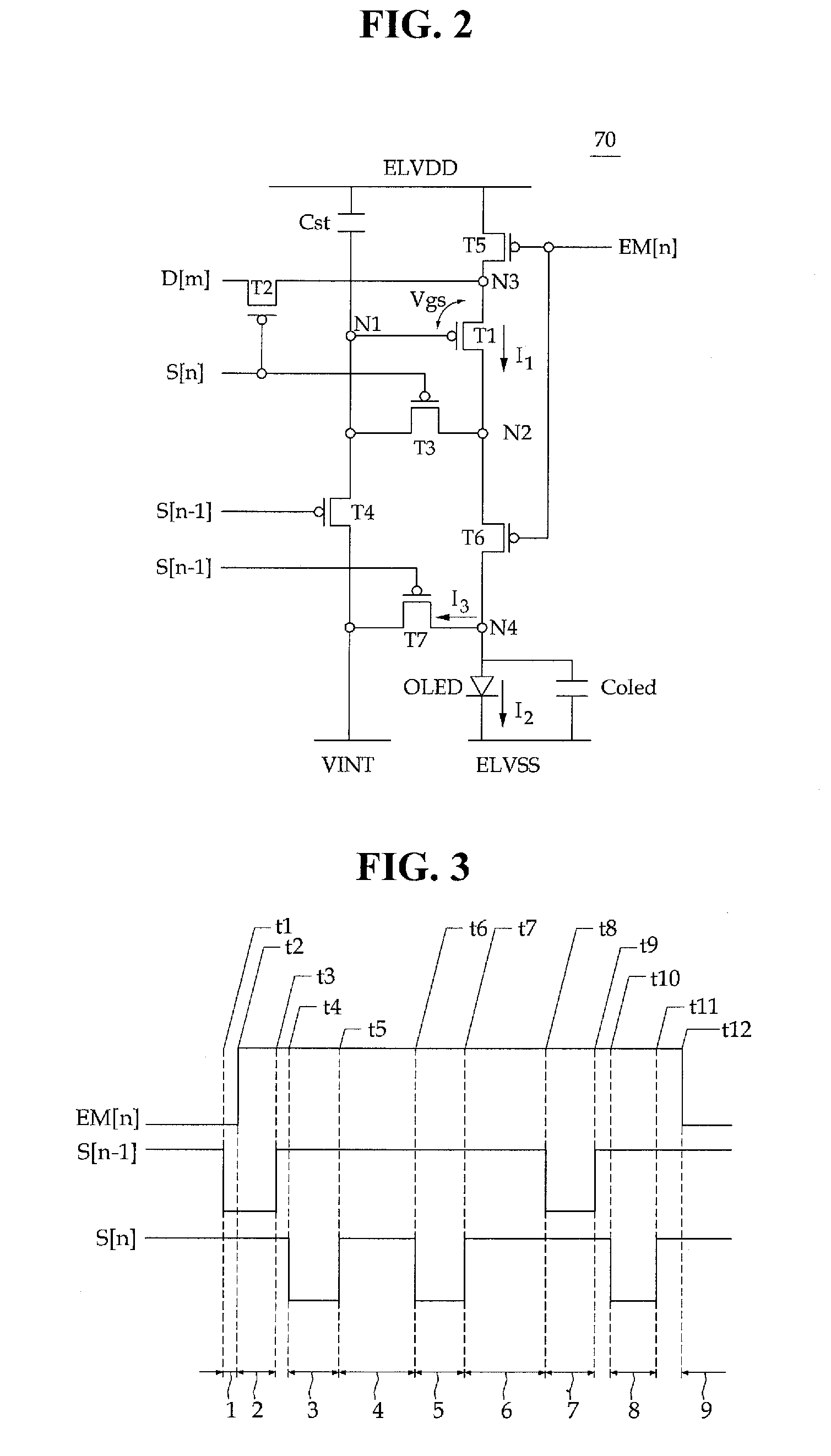
A method of driving a display device includes: applying a first voltage at the first transistor to turn on the first transistor; maintaining the first voltage at the first transistor; applying a second voltage lower than the first voltage at the first transistor; wherein the applying of the first voltage comprises switching the fourth transistor according to the second scan signal to couple the gate electrode of the first transistor to the third power source, and switching the fifth transistor according to the light emission control signal to couple the first electrode of the first transistor to the first power source, and the applying of the second voltage comprises switching the second transistor according to the first scan signal to couple the first electrode of the first transistor to the data line, and switching the third transistor according to the first scan signal to diode-couple the first transistor.

Description

CROSS-REFERENCE TO RELATED APPLICATION[0001]This application claims priority to and the benefit of Korean Patent Application No. 10-2013-0165538, filed on Dec. 27, 2013, with the Korean Intellectual Property Office, the disclosure of which is incorporated herein in its entirety by reference.BACKGROUND[0002]1. Field[0003]Embodiments of the present invention relate to a display device and a method for driving the same.[0004]2. Description of the Related Art[0005]Various types of flat panel displays (FPDs) that have reduced weight and volume compared to a cathode ray tube (CRT) are currently being developed. The FPDs include liquid crystal displays (LCDs), field emission displays (FEDs), plasma display panels (PDPs), organic light emitting diode (OLED) displays, and the like.[0006]Among the FPDs, the OLED display displays images using organic light emitting diodes (OLEDs) that generate light by recombining electrons and holes, and it is drawing attention owing to aspect such as short r...

Claims


Application Information

Patent Timeline
Patent Type & Authority Patents(United States)
IPC IPC(8): G09G3/30G09G3/32
CPCG09G3/3258G09G3/3233G09G3/3266G09G2300/0819G09G2300/0842G09G2300/0861G09G2310/0254G09G2320/045G09G2330/028G09G2360/08G09G2300/0426G09G3/32
Inventor LEEJEON, JINEOM, KI-MYEONGKIM, JI-HYE
Owner SAMSUNG DISPLAY CO LTD
Learn More