
Eureka
For R&D, Eureka makes reading and utilizing patents & technical documents easy.
Eureka AIR
Designed for self-driven R&D workflows. Generate viable solutions, solve complex R&D challenges, empower your innovation with AI.

Eureka Materials
Designed for material experts only. Revolutionize your material R&D, from search, analyze, to developing new materials.

TechResearch
Generate reliable direction feasibility study reports for your R&D in just a few steps.

TechSeek
Discover and master advanced knowledge NOW. Basics, ideas, possibilities, all at once.

TechMind
As an expert in R&D Theories, TechMind can generates customized viable solutions instantly.

TechRisk
Analyze your overall solution with one click, know your potential R&D risks in advance.

TechMonitor
Get weekly tech updates, stay abreast of the latest tech innovations and key insights.
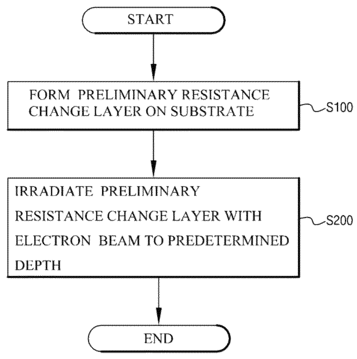
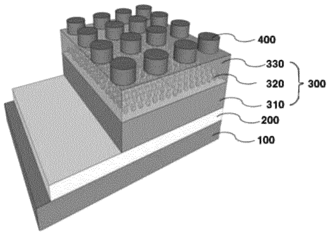
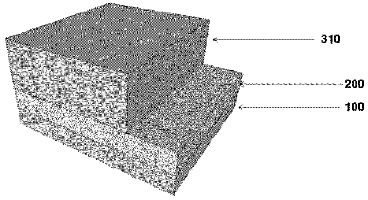
Method of manufacturing resistance change layer using irradiation of electron beam and resistive random access memory device using the same
a random access memory and resistance change technology, which is applied in semiconductor/solid-state device manufacturing, basic electric elements, electric apparatus, etc., can solve the problem that the charge trap type nand flash memory devices are difficult to be highly integrated any more, and achieve the effect of reducing the second resistance change layer
- Summary
- Abstract
- Description
- Claims
- Application Information
AI Technical Summary
Benefits of technology
Problems solved by technology
Method used
Image

Examples
manufacturing example 1
[0127]A glass-substrate / Pt / ZnO / ZnxO1-x / In—In2O3 core-shell structured quantum dot / ZnxO1-x / ZnO / Pt resistive random access memory device in accordance with an embodiment of the present invention was fabricated.
[0128]A Pt electrode was deposited on the glass substrate using a DC sputtering method.
[0129]Next, a ZnO thin film was deposited on the Pt electrode to have a thickness of 50 nm in an atmosphere of 10 sccm Ar at 70 W using a UHV sputtering method.
[0130]Next, a ZnxO1-x thin film was deposited to have a thickness of 50 nm in an atmosphere of 10 sccm Ar and 2 sccm O2.
[0131]Next, an Indium (In) thin film was deposited on the ZnxO1-x thin film to have a thickness of 5 nm in a vacuum of 5×10⁻⁶ Torr using a thermal evaporator.
[0132]Next, a ZnxO1-x thin film was deposited to have a thickness of 50 nm in an atmosphere of 10 sccm Ar and 2 sccm O2.
[0133]Then, a ZnO thin film was deposited to have a thickness of 50 nm an atmosphere of 10 sccm Ar at 70 W using a UHV sputtering method.
[0134]T...
manufacturing example 2
[0146]Electron beam irradiation was performed to a glass substrate / Pt / ZnO / ZnxO1-x / In—In2O3 core-shell structured quantum dot / ZnxO1-x / ZnO structure fabricated by the same method as in Manufacturing Example 1.
[0147]An electron beam was irradiated with energy of 0.2 MeV at a dose of 1×10¹⁴ e / cm2. In this case, an electron beam irradiation time was 20 seconds.
[0148]In conditions of the electron beam irradiation, the energy of electron beam irradiation was determined using Monte Carlo Simulation.
[0149]That is, although the electron beam with 0.2 MeV passes through the ZnO thin film, most of energy is lost in the ZnO thin film. That is, electrons having kinetic energy transfer the kinetic energy to a lattice inside the ZnO to form a defect structure in the ZnO lattice.
[0150]Here, the irradiation time of the electron beam is proportional to the amount of dose. The shape of the quantum dot formed inside and the structure of the ZnO thin film was confirmed using a cross-sectional TEM image.
[...
manufacturing example 3
[0154]Electron beam irradiation was performed like in the above-described Manufacturing Example 2. However, the electron beam was irradiated with energy of 0.2 MeV at a dose of 1×10¹⁵ e / cm2. In this case, an electron beam irradiation time was 60 seconds.
[0155]FIG. 18 is a high-resolution cross-sectional TEM image of the resistive random access memory device in accordance with Manufacturing Example 3.
[0156]Referring to FIG. 18, the shape of the quantum dot formed inside was maintained after the electron beam irradiation.
PUM
 Abstract
Description
Claims
Application Information
 - R&D Engineer
- R&D Manager
- IP Professional
- Industry Leading Data Capabilities
- Powerful AI technology
- Patent DNA Extraction
Browse by: Latest US Patents, China's latest patents, Technical Efficacy Thesaurus, Application Domain, Technology Topic, Popular Technical Reports.
© 2024 PatSnap. All rights reserved.Legal|Privacy policy|Modern Slavery Act Transparency Statement|Sitemap|About US| Contact US: help@patsnap.com