LCD device and manufacturing method thereof
a liquid crystal display and spacer technology, applied in non-linear optics, instruments, optics, etc., can solve problems such as display frame blues, change contrast or even view angle and quality of lcd
- Summary
- Abstract
- Description
- Claims
- Application Information
AI Technical Summary
Benefits of technology
Problems solved by technology
Method used
Image

Examples
Embodiment Construction
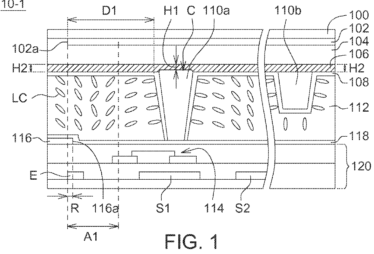
[0016]FIG. 1 shows a cross-sectional view of an LCD device 10-1 according to an embodiment of the invention. Referring to FIG. 1, the LCD device 10-1 comprises a first substrate 100, a light shielding layer 102, a color filtering layer 104, a first electrode 106, a first alignment layer 108, a main spacer 110a, an auxiliary spacer 110b, a liquid crystal layer 112, a transistor 114, a second electrode 116, a second alignment layer 118 and a second substrate 120.
[0017]As indicated in FIG. 1, the light shielding layer 102 may be disposed on the first substrate 100. The light shielding layer 102 can be a black matrix (BM) layer, a metal or non-metal opaque layer, and the light shielding layer 102 has an edge 102a. The color filtering layer 104 may be disposed on the light shielding layer 102 for selecting the range of wavelength of the light which could pass through. The color filtering layer 104 is a color filter (CF). In an embodiment, the color filtering layer 104 may selectively com...
PUM
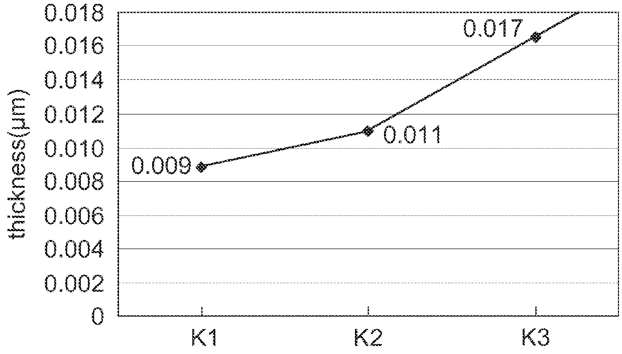
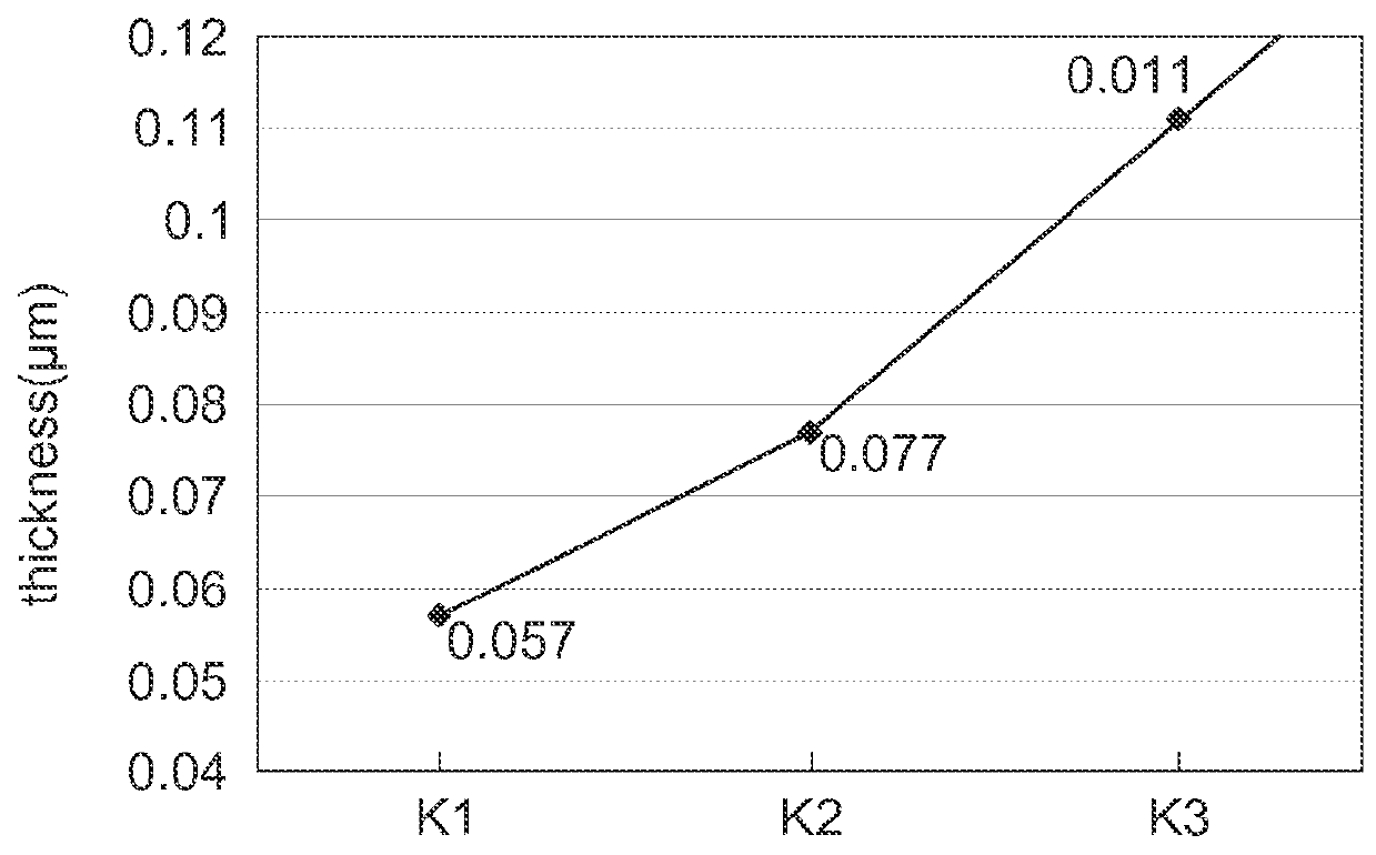
| Property | Measurement | Unit |
|---|---|---|
| thickness | aaaaa | aaaaa |
| thickness | aaaaa | aaaaa |
| distance | aaaaa | aaaaa |
Abstract
Description
Claims
Application Information