
Accessing an off-chip cache via silicon photonic waveguides

a silicon photonic waveguide and cache technology, applied in the field of cache implementation techniques, can solve the problems of introducing additional routing complexity, limited cache space available, non-uniform access times, etc., and achieve the effect of reducing the wire latency of cache access and uniform latency

Active Publication Date: 2016-07-12
ORACLE INT CORP
View PDF9 Cites 0 Cited by
  • Summary
  • Abstract
  • Description
  • Claims
  • Application Information

AI Technical Summary

Benefits of technology

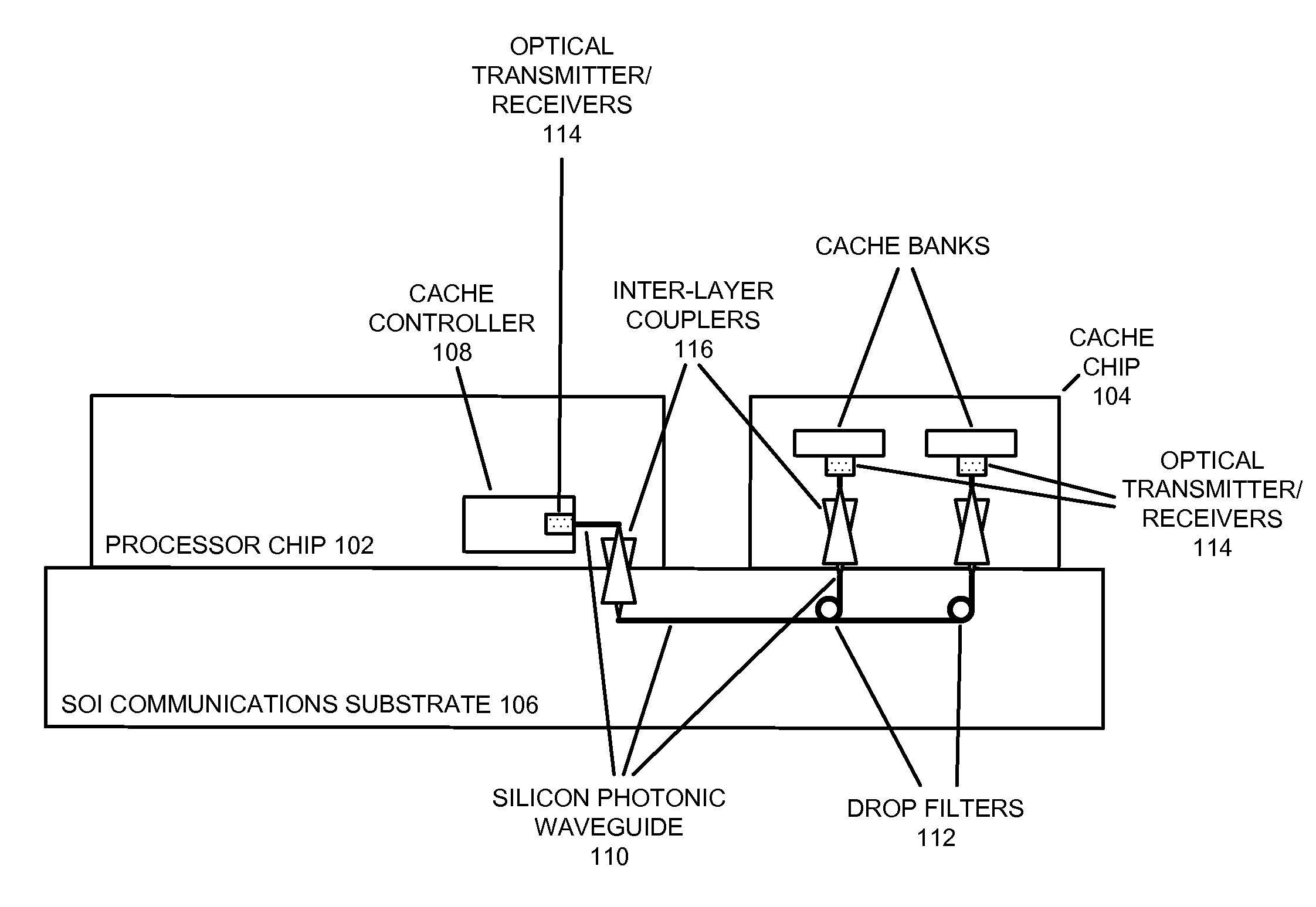
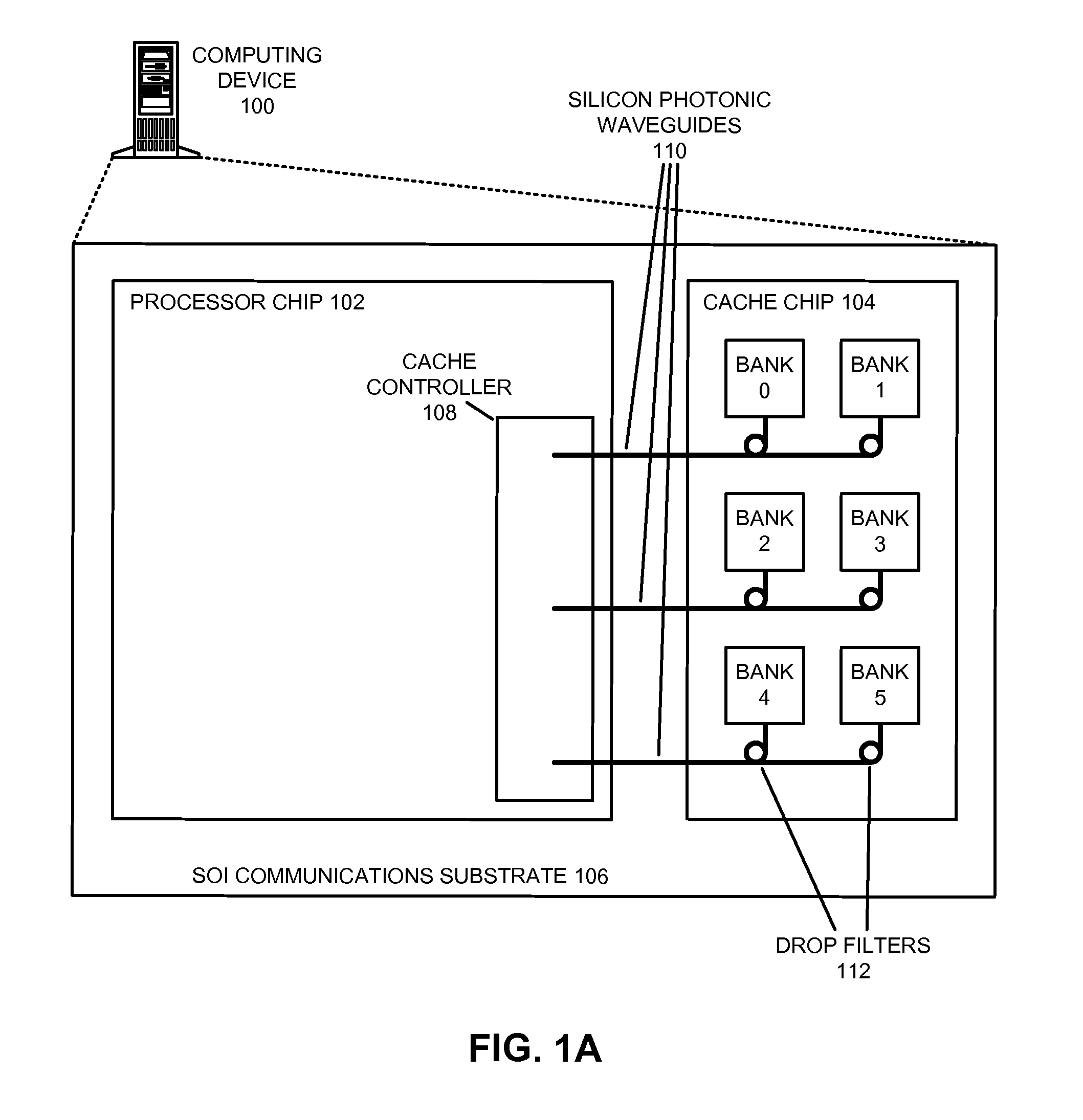
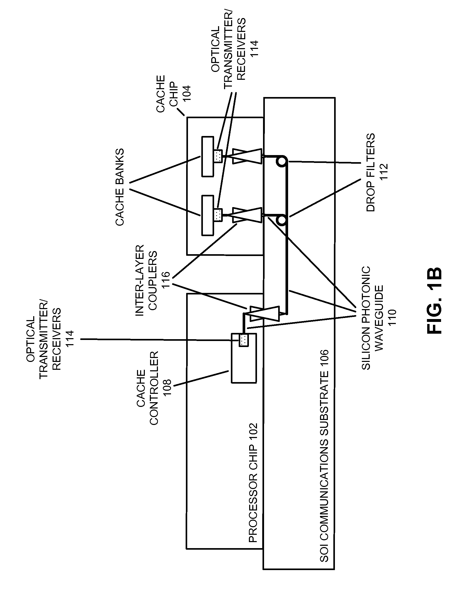
[0008]The disclosed embodiments provide a system in which a processor chip accesses an off-chip cache via silicon photonic waveguides. The system includes a processor chip and a cache chip that are both coupled to a communications substrate. The cache chip comprises one or more cache banks that receive cache requests from a structure in the processor chip optically via a silicon photonic waveguide. More specifically, the silicon photonic waveguide is comprised of waveguides in the processor chip, the communications substrate, and the cache chip, and forms an optical channel that routes an optical signal directly from the structure to a cache bank in the cache chip via the communications substrate. Transmitting optical signals from the processor chip directly to cache banks on the cache chip facilitates reducing the wire latency of cache accesses and allowing each cache bank on the cache chip to be accessed with uniform latency.

Problems solved by technology

However, in single-chip processor designs, the amount of space available for caches is limited by die size and the area required for the processor cores and other structures.
Large caches also suffer from significant wire delays, which can lead to non-uniform access times for different cache banks or may require the use of optimized wires that consume more area and introduce additional routing complexity.
Placing large caches on a separate chip reduces some area limitations, but off-chip electronic connections typically do not provide sufficient bandwidth for high-speed cache access.

Method used


Image

  • Accessing an off-chip cache via silicon photonic waveguides
  • Accessing an off-chip cache via silicon photonic waveguides
  • Accessing an off-chip cache via silicon photonic waveguides

Examples


Embodiment Construction

[0021]The following description is presented to enable any person skilled in the art to make and use the invention, and is provided in the context of a particular application and its requirements. Various modifications to the disclosed embodiments will be readily apparent to those skilled in the art, and the general principles defined herein may be applied to other embodiments and applications without departing from the spirit and scope of the present invention. Thus, the present invention is not limited to the embodiments shown, but is to be accorded the widest scope consistent with the principles and features disclosed herein.

[0022]The data structures and code described in this detailed description are typically stored on a non-transitory computer-readable storage medium, which may be any device or non-transitory medium that can store code and / or data for use by a computer system. The non-transitory computer-readable storage medium includes, but is not limited to, volatile memory,...


PUM


Abstract

The disclosed embodiments provide a system in which a processor chip accesses an off-chip cache via silicon photonic waveguides. The system includes a processor chip and a cache chip that are both coupled to a communications substrate. The cache chip comprises one or more cache banks that receive cache requests from a structure in the processor chip optically via a silicon photonic waveguide. More specifically, the silicon photonic waveguide is comprised of waveguides in the processor chip, the communications substrate, and the cache chip, and forms an optical channel that routes an optical signal directly from the structure to a cache bank in the cache chip via the communications substrate. Transmitting optical signals from the processor chip directly to cache banks on the cache chip facilitates reducing the wire latency of cache accesses and allowing each cache bank on the cache chip to be accessed with uniform latency.

Description

GOVERNMENT LICENSE RIGHTS[0001]This invention was made with United States Government support under Agreement No. HR0011-08-9-0001 awarded by the Defense Advanced Research Projects Administration (DARPA). The United States Government has certain rights in the invention.BACKGROUND[0002]1. Field of the Invention[0003]This disclosure generally relates to techniques for implementing off-chip caches for computer systems. More specifically, this disclosure relates to techniques for using a separate cache chip that is accessed using optical waveguides that connect directly to each cache bank.[0004]2. Related Art[0005]High instruction throughput in a processor typically involves rapid translation of virtual addresses and fast memory accesses. To achieve such throughput, the memory subsystem of the processor may include a number of specialized hardware structures, including multiple levels of caches. Such caching structures reduce the average latency of memory accesses.[0006]Most workloads ge...

Claims


Application Information

Patent Timeline
Patent Type & Authority Patents(United States)
IPC IPC(8): G06F12/00G06F12/08
CPCG06F12/0848G06F12/0893
Inventor KOKA, PRANAYMCCRACKEN, MICHAEL O.SCHWETMAN, JR., HERBERT D.HO, RONALD
Owner ORACLE INT CORP
Learn More