Laser processing apparatus and laser processing method using the same technical field

a laser processing and laser processing technology, applied in the direction of soldering apparatus, manufacturing tools,auxillary welding devices, etc., can solve the problems of reducing the reliability of electrical connections, reducing the accuracy of the position of holes, and reducing the number of operations. , the effect of minimizing the influence of movement on the processing accuracy

Active Publication Date: 2016-08-23
PANASONIC INTELLECTUAL PROPERTY MANAGEMENT CO LTD
View PDF19 Cites 3 Cited by
  • Summary
  • Abstract
  • Description
  • Claims
  • Application Information

AI Technical Summary

Benefits of technology

[0019]With a laser processing apparatus and a laser processing method according to the present invention, tensioning is not required even when laser-processing thin substrate material such as a prepreg sheet, thereby enabling laser processing while maintaining the dimensions of the substrate stably.
[0030]Further, only one-time setting of a workpiece to the laser processing apparatus enables laser processing through and non-through holes, thereby eliminating unevenness caused by positioning to improve the accuracy in laser processing position and significantly improving the productivity.

Problems solved by technology

However, if retaining the prepreg sheet in midair while tensioning it with a jig for pulling the ends of the sheet, a thin prepreg sheet with the resin partially hardening may undesirably change in its processing dimensions during laser processing.
Especially for a multilayer printed wiring board in which a prepreg sheet with a conductive paste filling a hole to be processed by laser used as an interlayer connector, deviation in the position of an interlayer conducting hole occurs due to a dimensional change and unevenness of the prepreg sheet, possibly decreasing the reliability in electrical connection.
However, the above-described conventional method results in executing setting of the laser processing apparatus twice for hole drilling in one sheet-like substrate, which may lower the accuracy in the position of holes, significantly decreasing the productivity for printed wiring boards.

Method used


Image

  • Laser processing apparatus and laser processing method using the same technical field
  • Laser processing apparatus and laser processing method using the same technical field
  • Laser processing apparatus and laser processing method using the same technical field

Examples


Embodiment Construction

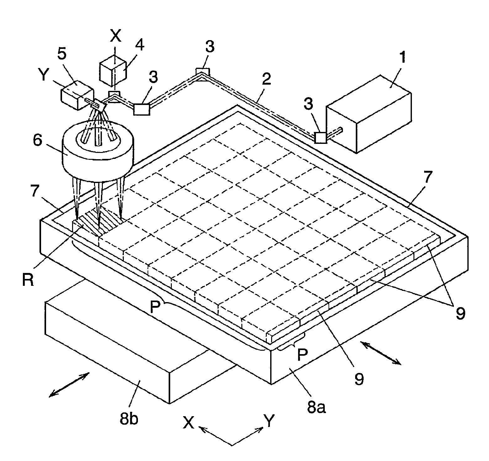
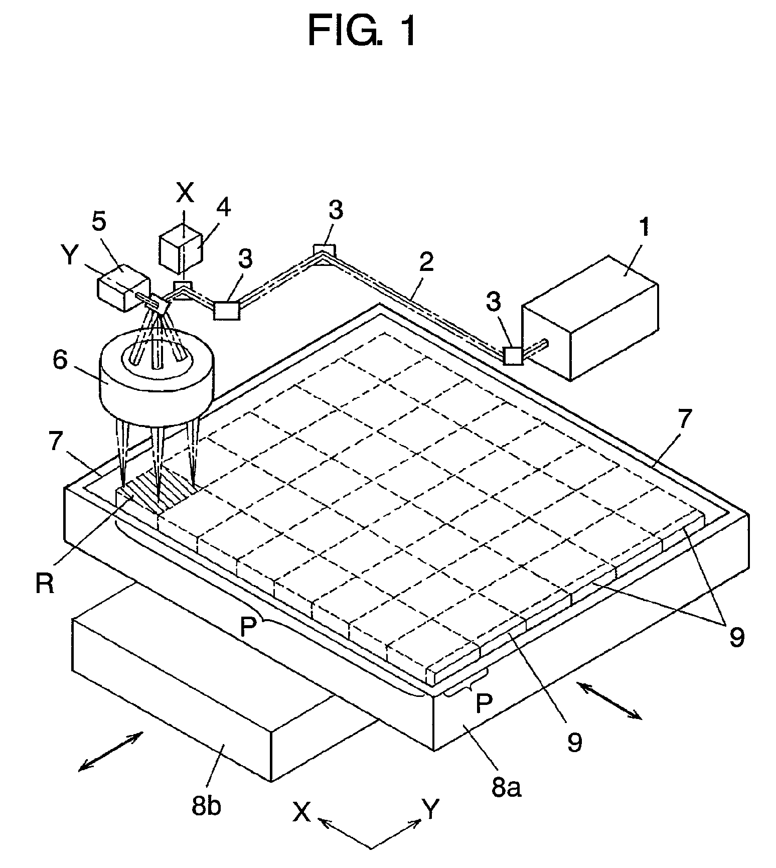
[0048]FIG. 1 illustrates the configuration of a laser processing apparatus according to the embodiment of the present invention. FIG. 2 is a schematic diagram of the XY table of the laser processing apparatus according to the same embodiment. In FIGS. 1, 2, the laser processing apparatus of the present invention includes laser oscillator 1, reflecting mirror 3, galvanometers 4, 5 with two-axis (X-Y) galvanometer mirror, and fθ lens 6. The operation of the apparatus and the configuration of its optical system such a path through which substrate 7 (i.e. workpiece) is irradiated with laser beam 2 emitted from laser oscillator 1 are roughly the same as those of a conventional one, thus their detailed description is omitted. Although this embodiment has one optical system to simplify the description and drawings, the invention is applicable to an apparatus with two optical systems (i.e. what is called a two-axis laser processing apparatus), where a branching means is provided between las...


PUM

PropertyMeasurementUnit
thicknessaaaaaaaaaa
areaaaaaaaaaaa
longitudinal lengthaaaaaaaaaa

Abstract

A laser processing apparatus is provided in which its XY table is composed of plural divided blocks vertically movable, at least one divided block is stopped while it is moving down, and a through hole is formed by irradiating a workpiece in an area corresponding to a position directly above the divided block with a laser beam.

Description

[0001]This application is a U.S. National Phase Application of PCT International Application PCT / JP2007 / 074498.TECHNICAL FIELD[0002]The present invention relates to a laser processing apparatus for processing (e.g. drilling) a workpiece such as a circuit substrate and to a method of the same.BACKGROUND ART[0003]FIG. 6 illustrates the configuration of a conventional laser processing apparatus. In FIG. 6, the laser processing apparatus drills a fine hole in a workpiece such as substrate 57 by irradiating the workpiece with a laser beam. A description is made for the configuration of the conventional laser processing apparatus.[0004]First, laser beam 52 is emitted from laser oscillator 51, direction-converted by reflecting mirror 53a, and then is led from reflecting mirror 53b, 53c toward galvanometers 54, 55 including a two-axis (X, Y) galvanometer mirror. Then, laser beam 52 is launched into fθ lens 56 with its irradiation direction changed by the operation of galvanometers 54, 55 an...

Claims


Application Information

Patent Timeline
Patent Type & Authority Patents(United States)
IPC IPC(8): B23K26/00H05K3/00B23K26/02B23K26/08B23K37/04B23K26/40B23K26/142B23K26/382
CPCB23K26/0853B23K37/0408H05K3/0032B23K26/082B23K26/382B23K26/40B23K26/402H05K2203/0165H05K2203/082B23K2203/08B23K2203/16B23K2201/35B23K2203/50B23K2203/42B23K2203/38B23K2103/12B23K2103/166B23K2103/50B23K2101/35B23K2103/08B23K2103/16B23K2103/38B23K2103/42B23K26/08B23K26/035
Inventor NAKAGAWA, YOSHINORIHARA, MITSUO
Owner PANASONIC INTELLECTUAL PROPERTY MANAGEMENT CO LTD
Why Eureka
Try Eureka