Semiconductor device

a technology of semiconductors and semiconductors, applied in the field of semiconductor devices, can solve the problems of less suitable for high-speed operation increase in memory capacity, and less suitable for memory expansion than a binary memory, and achieve the effect of high convenience and new structur

Active Publication Date: 2016-09-06
SEMICON ENERGY LAB CO LTD
View PDF156 Cites 1 Cited by
  • Summary
  • Abstract
  • Description
  • Claims
  • Application Information

AI Technical Summary

Benefits of technology

[0010]In view of the above, an object of one embodiment of the present invention is to provide a semiconductor device or the like that has a novel structure and achieves a higher degree of convenience. An object of one embodiment of the present invention is to provide a semiconductor device or the like that has a novel structure and has compatibility between a binary memory and a multilevel memory. An object of one embodiment of the present invention is to provide a semiconductor device or the like that has a novel structure and can be additionally provided with a binary memory or a multilevel memory after being mounted on a substrate. An object of one embodiment of the present invention is to provide a semiconductor device or the like which has a novel structure and in which a memory to be used can switch between a binary memory and a multilevel memory depending on the application. An object of one embodiment of the present invention is to provide a semiconductor device or the like which has a novel structure and in which a memory to be used can switch between a binary memory and a multilevel memory without an increase in circuit size. An object of one embodiment of the present invention is to provide a semiconductor device or the like which has a novel structure and in which the number of levels of data that a multilevel memory can store can be changed without an increase in circuit size. An object of one embodiment of the present invention is to provide a semiconductor device or the like that has a novel structure and is capable of changing the operating speed. An object of one embodiment of the present invention is to provide a semiconductor device or the like which has a novel structure and in which the off-state current is low. An object of one embodiment of the present invention is to provide a semiconductor device or the like with a novel structure with low power consumption. An object of one embodiment of the present invention is to provide a semiconductor device or the like with a novel structure with high reliability. An object of one embodiment of the present invention is to provide a semiconductor device or the like with a novel structure.
[0018]In one embodiment of the present invention, a semiconductor device that has a novel structure and achieves a high degree of convenience can be provided.

Problems solved by technology

A binary memory particularly needs to operate at high speed to store data temporarily and is less suitable for an increase in memory capacity than a multilevel memory.
A multilevel memory particularly requires an increase in memory capacity for storing a large amount of data and is less suitable for high-speed operation than a binary memory.
Since the compatibility between the binary memory and the multilevel memory is not maintained after the memories are mounted on the printed circuit board, it is difficult to switch the memories depending on the application, and the convenience is hampered as a result.

Method used


Image

  • Semiconductor device
  • Semiconductor device
  • Semiconductor device

Examples


embodiment 2

(Embodiment 2)

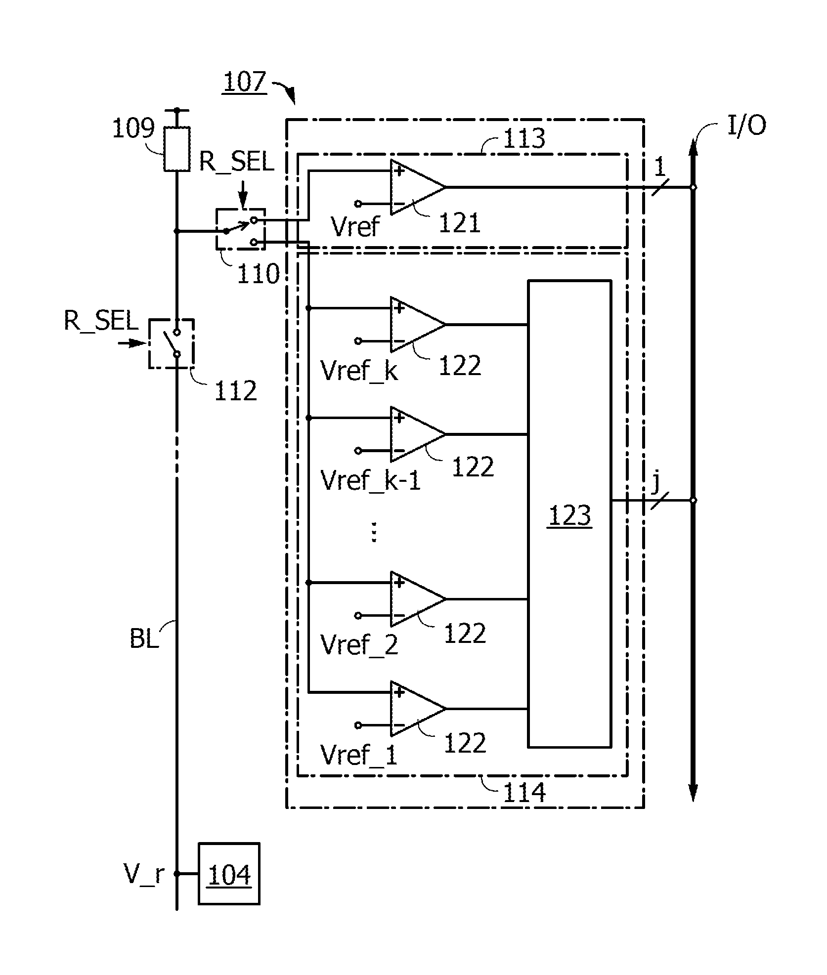
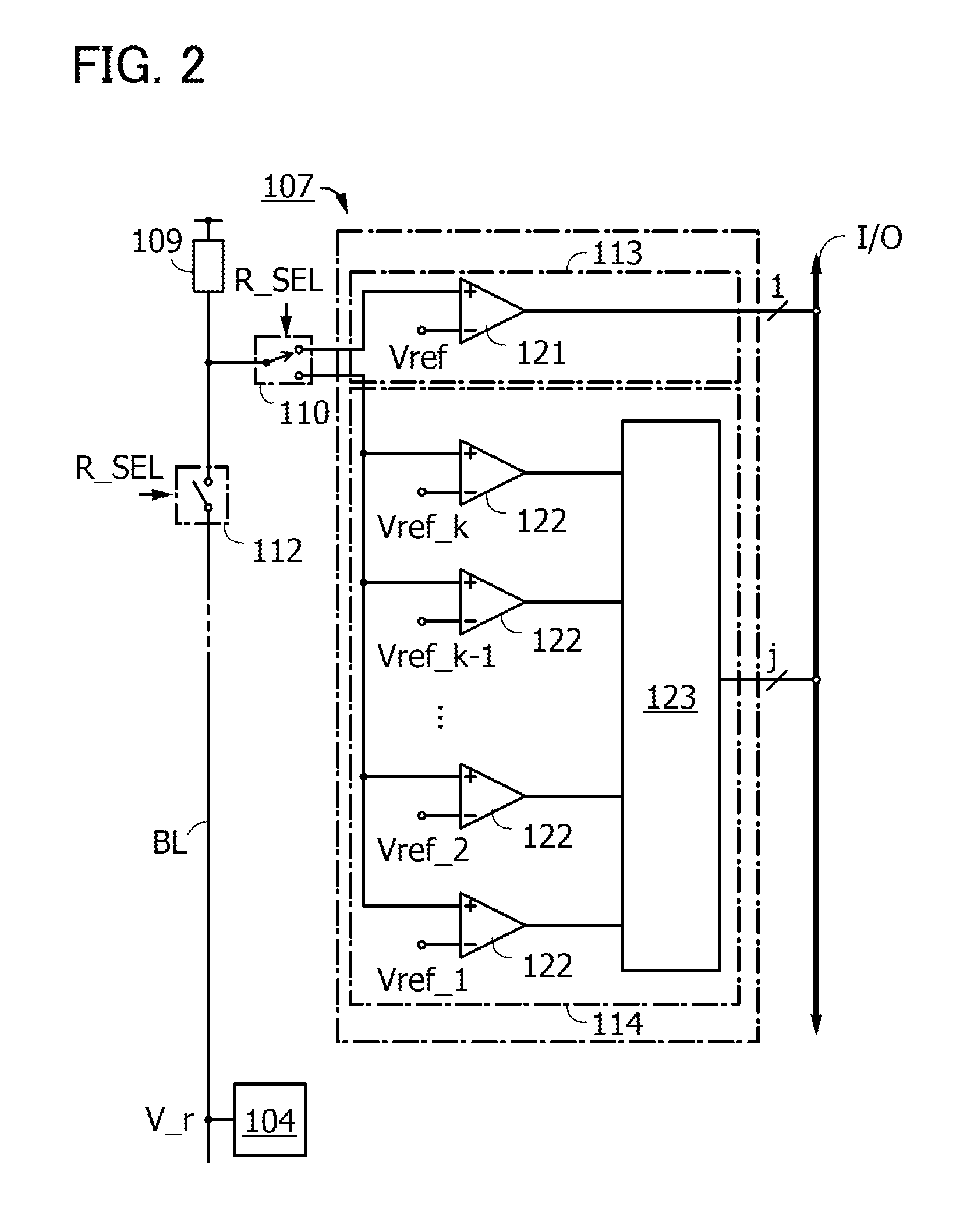
[0113]In Embodiment 2, a structure example of the reading circuit described in Embodiment 1 will be described with reference to FIG. 2.

[0114]The block diagram of the reading circuit 107 in FIG. 2 shows the reading circuit 113, the reading circuit 114, a comparator 121, comparators 122, and an arithmetic circuit 123. FIG. 2 also shows the memory cell 104, the load 109, the read switching circuit 110, the read switching switch 112, and the input / output unit I / O.

[0115]The reading circuit 113 can compare the levels of the reference voltage Vref and a read data voltage that is input to the comparator 121 in response to switching of the read switching circuit 110 and the read switching switch 112. As the determination result of the comparison by the reading circuit 113, 1-bit data having H level or L level, that is, 1-bit data of data ‘0’ or data ‘1’ is output to the input / output unit I / O.

[0116]In the reading circuit 114, a read data voltage input by switching of the read sw...

embodiment 3

(Embodiment 3)

[0121]In Embodiment 3, a structure example of the writing circuit described in Embodiment 1 will be described with reference to FIG. 3.

[0122]The block diagram of the writing circuit 108 in FIG. 3 shows a writing circuit 131 and a writing circuit 132. FIG. 3 also shows the memory cell 104, the write switching circuit 111, the voltage generator circuit 106, and the input / output unit I / O.

[0123]The writing circuit 131 is supplied with data through the input / output unit I / O and outputs a voltage corresponding to the data to the memory cell 104 through the bit line BL. For example, the writing circuit 131 is supplied with voltages V_1 and V_k serving as write data voltages for binary data from the voltage generator circuit 106, and outputs one of the voltages in accordance with the data.

[0124]The writing circuit 132 is supplied with data through the input / output unit I / O and outputs a voltage corresponding to the data to the memory cell 104 through the bit line BL. For examp...

embodiment 4

(Embodiment 4)

[0128]In Embodiment 4, structure examples of the memory cell described in Embodiment 1 will be described with reference to FIGS. 4A to 4C and FIGS. 5A and 5B.

[0129]The circuit diagram of the memory cell 104 in FIG. 4A shows a transistor 141, a transistor 142, a capacitor 143, the bit line BL, the source line SL, the word line WL, and the capacitor word line CL. FIG. 4A also shows a node Node_M connected to the transistor 141, the transistor 142, and the capacitor 143. Although the transistors 141 and 142 are n-channel transistors in the following description, at least one of the transistors 141 and 142 may be a p-channel transistor.

[0130]The transistor 141 has a function of controlling supply of a write data voltage of the bit line BL to the node Node_M when the voltage level of a word signal supplied to the word line WL is at H level. The transistor 141 also has a function of preventing a variation in the potential of the node Node_M due to leakage of charge held at t...


PUM


Abstract

To provide a semiconductor device that has a novel structure and achieves a higher degree of convenience, the semiconductor device is configured to include a memory cell that stores binary data or multilevel data, and a reading circuit that reads the data stored in the memory cell and transfers the data to the outside. The reading circuit includes a first reading circuit for reading binary data and a second reading circuit for reading multilevel data.

Description

BACKGROUND OF THE INVENTION[0001]1. Field of the Invention[0002]The present invention relates to an object (a product including a machine, a manufacture, and a composition of matter) and a method (a process including a simple method and a production method). In particular, one embodiment of the present invention relates to a semiconductor device, a display device, a light-emitting device, a driving method thereof, or a manufacturing method thereof. One embodiment of the present invention particularly relates to, for example, a semiconductor device or a driving method thereof.[0003]2. Description of the Related Art[0004]Semiconductor devices including elements using semiconductor properties have attracted attention. An example of an element using semiconductor properties is a transistor. A transistor is used in a liquid crystal display device, a memory device, and the like.[0005]Although silicon (Si) is widely known as a semiconductor material used for a transistor, an oxide semicond...

Claims


Application Information

Patent Timeline
Patent Type & Authority Patents(United States)
IPC IPC(8): G11C16/26G11C11/405G11C11/4076G11C11/56
CPCG11C11/405G11C11/4076G11C11/56G11C11/5621G11C11/5642G11C2211/5641
Inventor YAMAZAKI, SHUNPEIKOYAMA, JUN
Owner SEMICON ENERGY LAB CO LTD
Why Eureka
Try Eureka