Semiconductor device

a semiconductor film and semiconductor technology, applied in the field of objects, can solve the problems of electrical characteristics that vary among the transistors, and achieve the effects of reducing power consumption, reducing electrical characteristics, and suppressing the change in electrical characteristics of the transistor including the oxide semiconductor film

Active Publication Date: 2016-09-13
SEMICON ENERGY LAB CO LTD
View PDF129 Cites 10 Cited by
  • Summary
  • Abstract
  • Description
  • Claims
  • Application Information

AI Technical Summary

Problems solved by technology

Further, there is a problem in that electrical characteristics vary among the transistors.

Method used


Image

  • Semiconductor device
  • Semiconductor device
  • Semiconductor device

Examples


embodiment 1

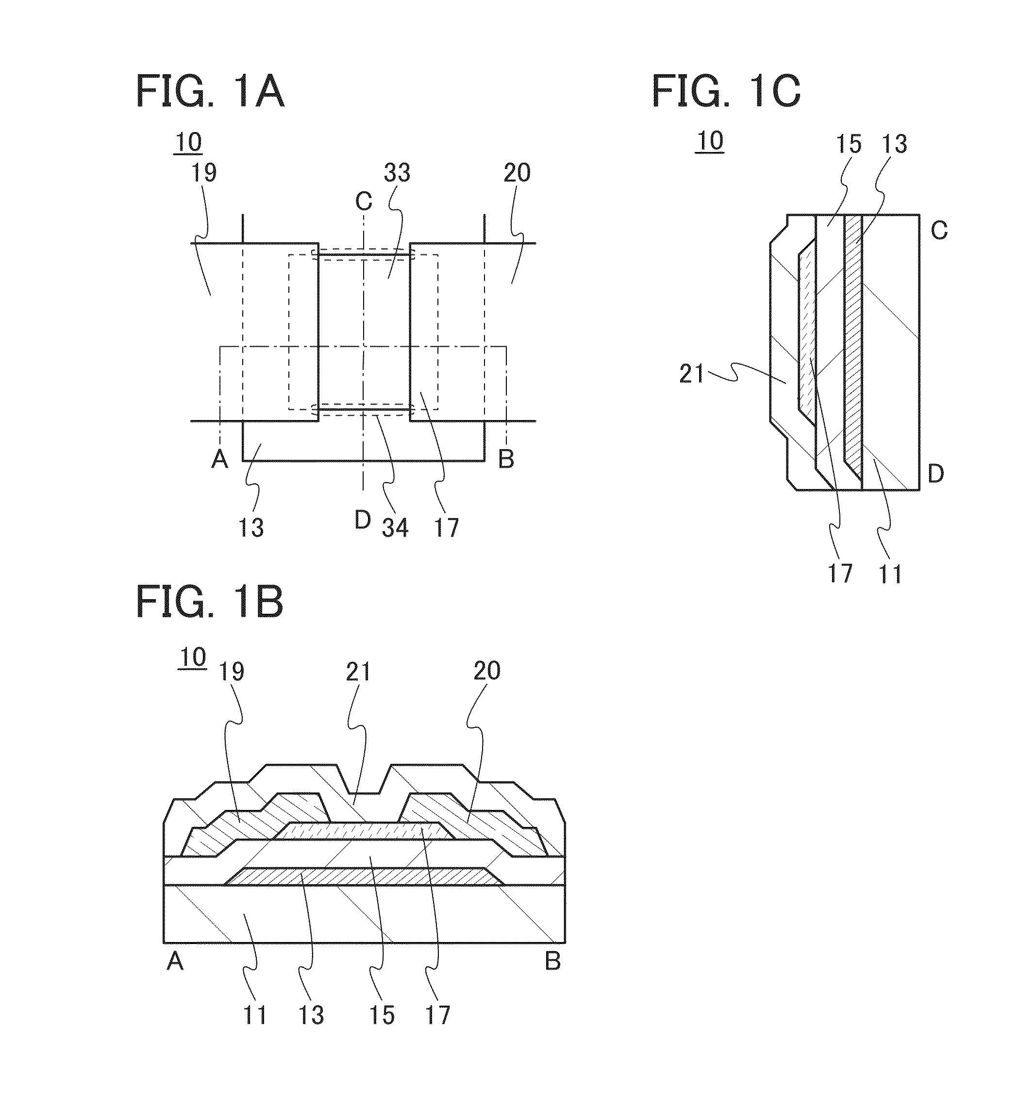
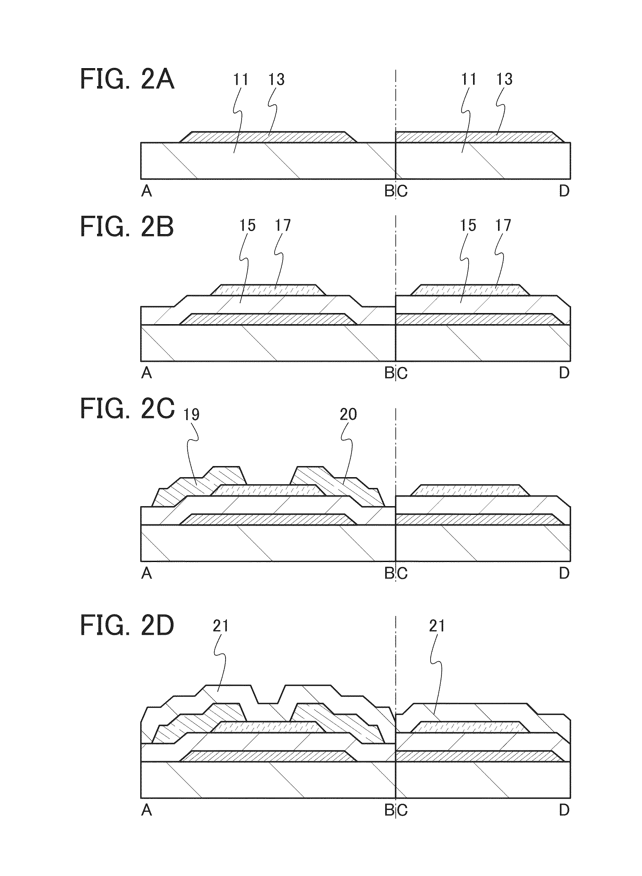
[0080]In this embodiment, a semiconductor device of one embodiment of the present invention and a method for manufacturing the semiconductor device are described with reference to drawings. A transistor 10 described in this embodiment has a bottom-gate structure.

[0081]FIGS. 1A to 1C are a top view and cross-sectional views of the transistor 10 included in a semiconductor device. FIG. 1A is a top view of the transistor 10, FIG. 1B is a cross-sectional view taken along dashed-dotted line A-B in FIG. 1A, and FIG. 1C is a cross-sectional view taken along dashed-dotted line C-D in FIG. 1A. Note that in FIG. 1A, a substrate 11, a gate insulating film 15, a protective film 21, and the like are omitted for simplicity.

[0082]The transistor 10 illustrated in FIGS. 1A to 1C includes a gate electrode 13 over the substrate 11, the gate insulating film 15 over the substrate 11 and the gate electrode 13, an oxide semiconductor film 17 overlapping with the gate electrode 13 with the gate insulating ...

modification example 3

[0180]Modification examples of the transistor 10 described in Embodiment 1 are described with reference to FIGS. 5A to 5C. The transistor 10 described in Embodiment 1 includes one gate electrode; in contrast, a transistor 10e described in this modification example includes two gate electrodes with an oxide semiconductor film interposed between the gate electrodes.

[0181]A top view and cross-sectional views of the transistor 10e included in a semiconductor device are illustrated in FIGS. 5A to 5C. FIG. 5A is a top view of the transistor 10e, FIG. 5B is a cross-sectional view taken along dashed-dotted line A-B in FIG. 5A, and FIG. 5C is a cross-sectional view taken along dashed-dotted line C-D in FIG. 5A. Note that in FIG. 5A, the substrate 11, the gate insulating film 15, the protective film 21, and the like are omitted for simplicity.

[0182]The transistor 10e illustrated in FIGS. 5B and 5C is a channel-etched transistor including the gate electrode 13 over the substrate 11; the gate i...

modification example 4

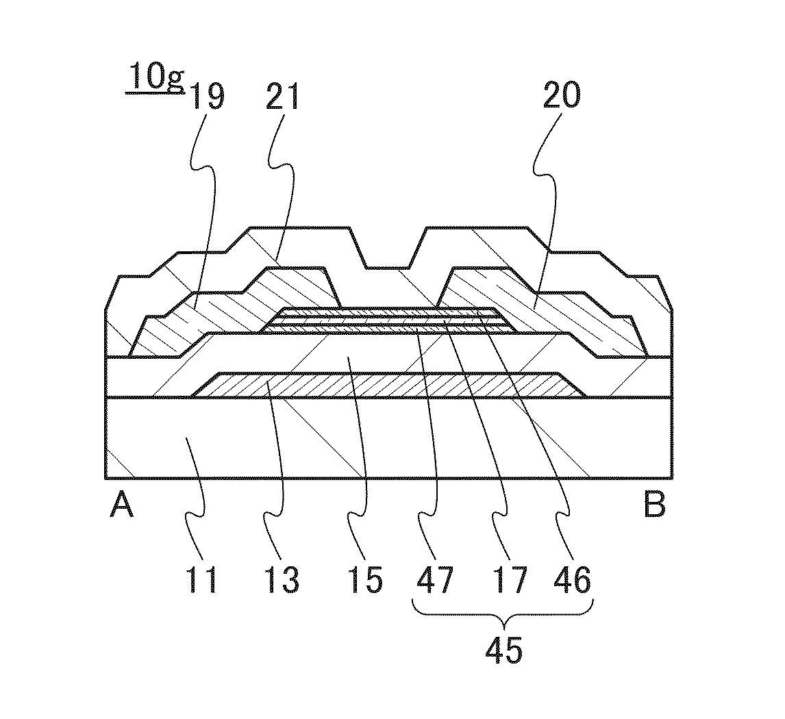
[0185]Modification examples of the transistor 10 described in Embodiment 1 are described with reference to FIGS. 6A to 6D and FIGS. 7A to 7C. The transistor 10 described in Embodiment 1 includes the single-layer oxide semiconductor film; in contrast, transistors 10f and 10g described in this modification example each includes a multi-layer film.

[0186]FIGS. 6A to 6C are a top view and cross-sectional views of the transistor 10f included in a semiconductor device. FIG. 6A is a top view of the transistor 10f, FIG. 6B is a cross-sectional view taken along dashed-dotted line A-B in FIG. 6A, and FIG. 6C is a cross-sectional view taken along dashed-dotted line C-D in FIG. 6A. Note that in FIG. 6A, the substrate 11, the gate insulating film 15, the protective film 21, and the like are omitted for simplicity.

[0187]The transistor 10f illustrated in FIG. 6A includes a multilayer film 45 overlapping with the gate electrode 13 with the gate insulating film 15 provided therebetween, and the pair ...


PUM


Abstract

In a semiconductor device using a transistor including an oxide semiconductor, a change in electrical characteristics is suppressed and reliability is improved. The semiconductor device includes a gate electrode over an insulating surface; an oxide semiconductor film overlapping with the gate electrode; a gate insulating film that is between the gate electrode and the oxide semiconductor film and in contact with the oxide semiconductor film; a protective film in contact with a surface of the oxide semiconductor film that is an opposite side of a surface in contact with the gate insulating film; and a pair of electrodes in contact with the oxide semiconductor film. The spin density of the gate insulating film or the protective film measured by electron spin resonance spectroscopy is lower than 1×10¹⁸ spins / cm3, preferably higher than or equal to 1×10¹⁷ spins / cm3 and lower than 1×10¹⁸ spins / cm3.

Description

BACKGROUND OF THE INVENTION[0001]1. Field of the Invention[0002]The present invention relates to an object, a method, or a manufacturing method. In addition, the present invention relates to a process, a machine, manufacture, or a composition of matter. In particular, the present invention relates to a semiconductor device, a display device, a light-emitting device, a power storage device, a driving method thereof, or a manufacturing method thereof. Furthermore in particular, the present invention relates to a semiconductor device including a field-effect transistor.[0003]In this specification and the like, a semiconductor device generally means a device that can function by utilizing semiconductor characteristics. A semiconductor element such as a transistor, a semiconductor circuit, an arithmetic device, and a memory device are each one embodiment of a semiconductor device. An imaging device, a display device, a liquid crystal display device, a light-emitting device, an electro-op...

Claims


Application Information

Patent Timeline
Patent Type & Authority Patents(United States)
IPC IPC(8): H01L29/66H01L29/12H01L29/10H01L29/786H01L29/49H01L29/24
CPCH01L29/7869H01L29/24H01L29/4908H01L29/78606H01L27/1225H01L29/045H01L29/66969H01L29/78696
Inventor MIYANAGA, AKIHARUHOSAKA, YASUHARUOBONAI, TOSHIMITSUKOEZUKA, JUNICHINAKASHIMA, MOTOKITAKAHASHI, MASAHIROADACHI, SHUNSUKEHIROHASHI, TAKUYA
Owner SEMICON ENERGY LAB CO LTD
Why Eureka
Try Eureka