Display substrate, manufacturing method thereof and flexible display device

a flexible display device and substrate technology, applied in the field of display substrates, can solve the problems of affecting the performance of tft, affecting the reliability and a variety of vulnerable members on the flexible base substrate of the flexible display device are liable to be damaged, so as to improve the reliability of the display substra

Active Publication Date: 2016-09-13
BOE TECH GRP CO LTD
View PDF11 Cites 1 Cited by
  • Summary
  • Abstract
  • Description
  • Claims
  • Application Information

AI Technical Summary

Benefits of technology

[0020]According to the display substrate and the flexible display device provided by the present invention, since the stress absorption layer is only arranged below the vulnerable member, and no stress absorption layer is arranged on other positions, stress generated during bending may be dispersed through the stress absorption layer to avoid stress concentration at the vulnerable member (namely, at the stress absorption layer), in order to protect the vulnerable member (e.g., TFT) from being damaged to improve the reliability of the display substrate and the flexible display device.

Problems solved by technology

Stress aggregation will be generated during bending, and with the increase of the number of bending operations, various vulnerable members on the flexible base substrate of the flexible display device are liable to be damaged.
For example, due to the stress aggregation during bending, the film layers of the thin film transistor (TFT) as a vulnerable member are likely to be fractured, which will affect the performance of the TFT and thus affect the reliability of the flexible display device.

Method used


Image

  • Display substrate, manufacturing method thereof and flexible display device
  • Display substrate, manufacturing method thereof and flexible display device
  • Display substrate, manufacturing method thereof and flexible display device

Examples


embodiment 1

[0040

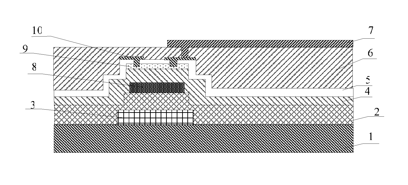
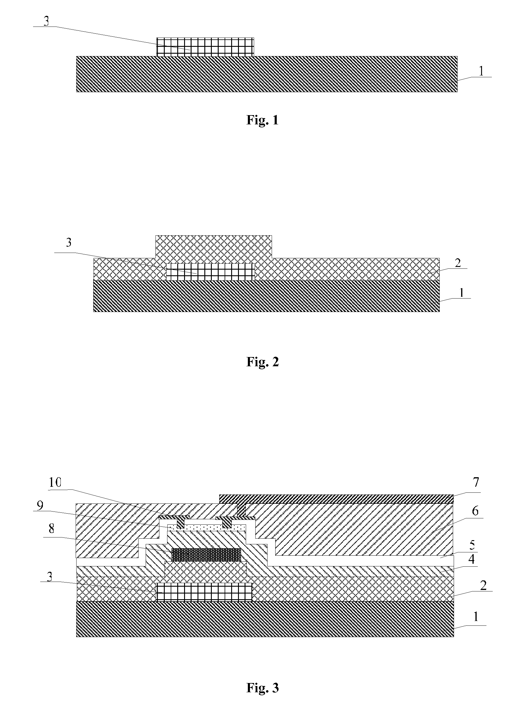
[0041]As shown in FIG. 1 to FIG. 3, this embodiment provides a display substrate, including a polyimide (PI) base substrate 1 and a TFT (used as an example of a vulnerable member) arranged on the PI base substrate, wherein a stress absorption layer 3 is arranged between the PI base substrate 1 and the TFT; the stress absorption layer 3 is formed by a patterning process, for example, the stress absorption layer 3 is formed by performing a patterning process by adopting a mask plate corresponding to the shape of the TFT.

[0042]As shown in FIG. 3, the projection of the TFT on the PI base substrate 1 is within the projection region of the stress absorption layer 3 on the PI base substrate 1. Preferably, the projection of the TFT on the base substrate coincides with the projection of the stress absorption layer 3 on the base substrate, namely, the stress absorption layer 3 is only arranged below the TFT. Therefore, stress generated when the display substrate is bent may be dispersed ...

embodiment 2

[0059

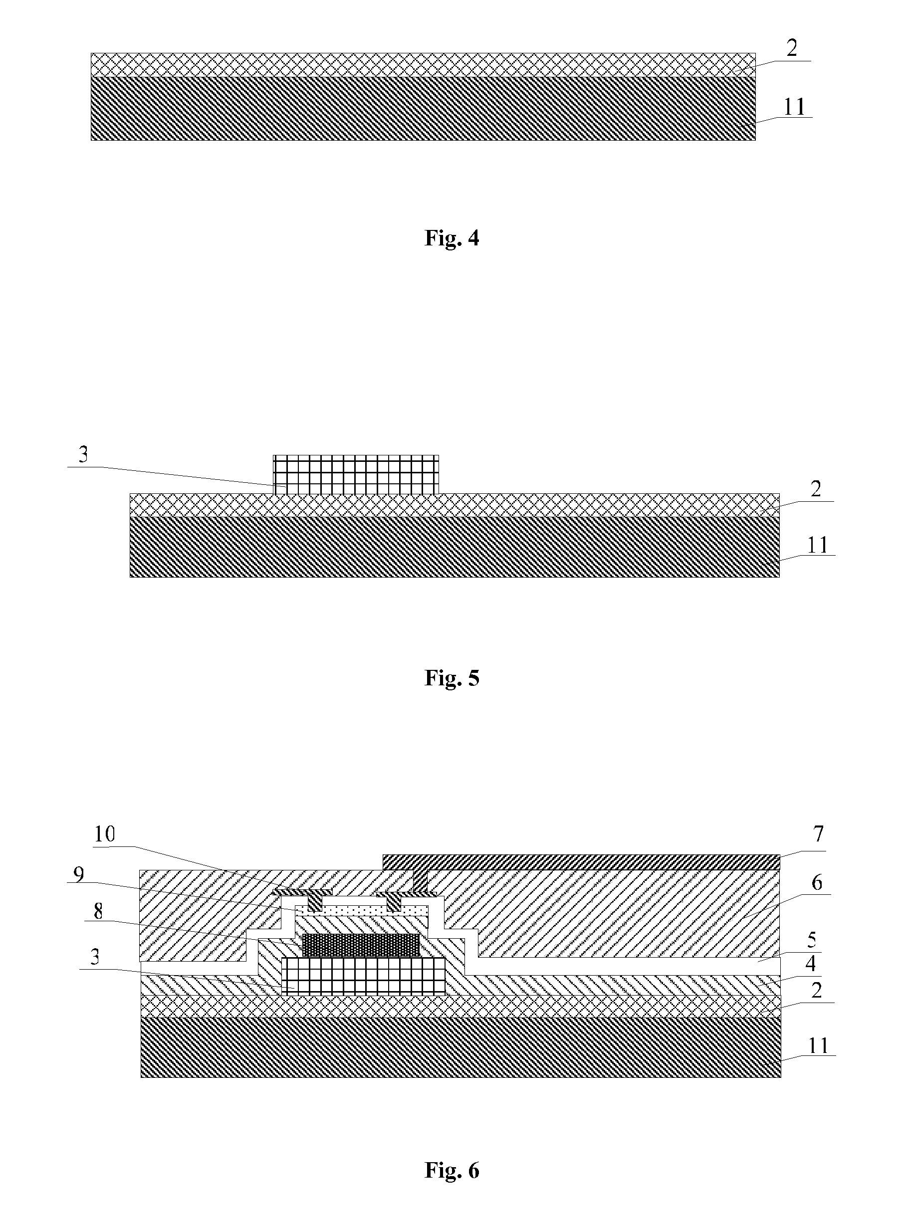
[0060]As shown in FIG. 4 to FIG. 6, this embodiment provides a display substrate, including a polyethylene glycol terephthalate (PET) base substrate 11 and a TFT (used as an example of a vulnerable member) arranged on the PET base substrate 11, wherein a stress absorption layer 3 is arranged between the PET base substrate 11 and the TFT; the stress absorption layer 3 is formed by a patterning process, for example, the stress absorption layer 3 is formed by performing a patterning process by adopting a mask plate corresponding to the shape of the TFT (used as the example of the vulnerable member).

[0061]As shown in FIG. 6, the projection of the TFT on the PET base substrate 11 is within the projection region of the stress absorption layer 3 on the PET base substrate 11. Preferably, the projection of the TFT on the base substrate coincides with the projection of the stress absorption layer 3 on the base substrate. The stress absorption layer 3 is not arranged on part of the PI bas...

embodiment 3

[0078

[0079]This embodiment provides a flexible display device, including the above-mentioned display substrate and other necessary assemblies. Preferably, the display substrate included in the flexible display device is a flexible organic light emitting diode display substrate.


PUM


Abstract

The invention provides a display substrate, a manufacturing method thereof and a flexible display device. The display substrate in the present invention includes a base substrate and a vulnerable member arranged on the base substrate, as well as a stress absorption layer arranged between the base substrate and the vulnerable member, wherein the projection of the vulnerable member on the base substrate is within the projection region of the stress absorption layer on the base substrate; the stress absorption layer is not arranged on part of the base substrate. Since the display substrate and the flexible display device provided by the present invention are provided with the stress absorption layer, stress generated during bending may be dispersed through the stress absorption layer to protect the vulnerable member from being damaged, so as to improve the reliability of the display substrate and the flexible display device.

Description

[0001]This is a National Phase Application filed under 35 U.S.C. 371 as a national stage of PCT / CN2014 / 078013, filed May 21, 2014, and claims priority benefit from Chinese Application No. 201310475753.3, filed Oct. 12, 2013, the content of each of which is hereby incorporated by reference in its entirety.FIELD OF THE INVENTION[0002]The present invention belongs to the field of display technology, and particularly relates to a display substrate, a manufacturing method thereof and a flexible display device containing the display substrate.BACKGROUND OF THE INVENTION[0003]Flexible display technology is a forward-looking technology which is popular in recent years, and a flexible display device is light and thin, bendable and even curlable and good in mechanical properties, thus attracting more and more attention of people. The flexible display device includes a display substrate, wherein the display substrate includes a base substrate and a structure on the base substrate, the base sub...

Claims


Application Information

Patent Timeline
Patent Type & Authority Patents(United States)
IPC IPC(8): H01L27/00H01L29/786H01L51/00H01L29/00H01L27/12H01L27/32
CPCH01L51/0097H01L27/1218H01L29/78603H01L51/0001H01L27/3244H01L2251/10H01L2251/5338Y02E10/549H10K59/12H10K77/111H10K2102/311H10K71/00
Inventor SHI, LINGLI, YUNFEINAGAYAMA, KAZUYOSHI
Owner BOE TECH GRP CO LTD
Why Eureka
Try Eureka