Systems and methods to mitigate program gate disturb in split-gate flash cell arrays

a technology of split-gate flash cell arrays and system and method, applied in information storage, static storage, instruments, etc., can solve the problem of high voltage being applied to other control gates within the array

Active Publication Date: 2016-09-20
NXP USA INC
View PDF11 Cites 0 Cited by
  • Summary
  • Abstract
  • Description
  • Claims
  • Application Information

AI Technical Summary

Problems solved by technology

However, this may result in high voltages being applied to other control gates within the array even when the particular memory cell is not the subject of the instant operation.

Method used


Image

  • Systems and methods to mitigate program gate disturb in split-gate flash cell arrays
  • Systems and methods to mitigate program gate disturb in split-gate flash cell arrays
  • Systems and methods to mitigate program gate disturb in split-gate flash cell arrays

Examples


Embodiment Construction

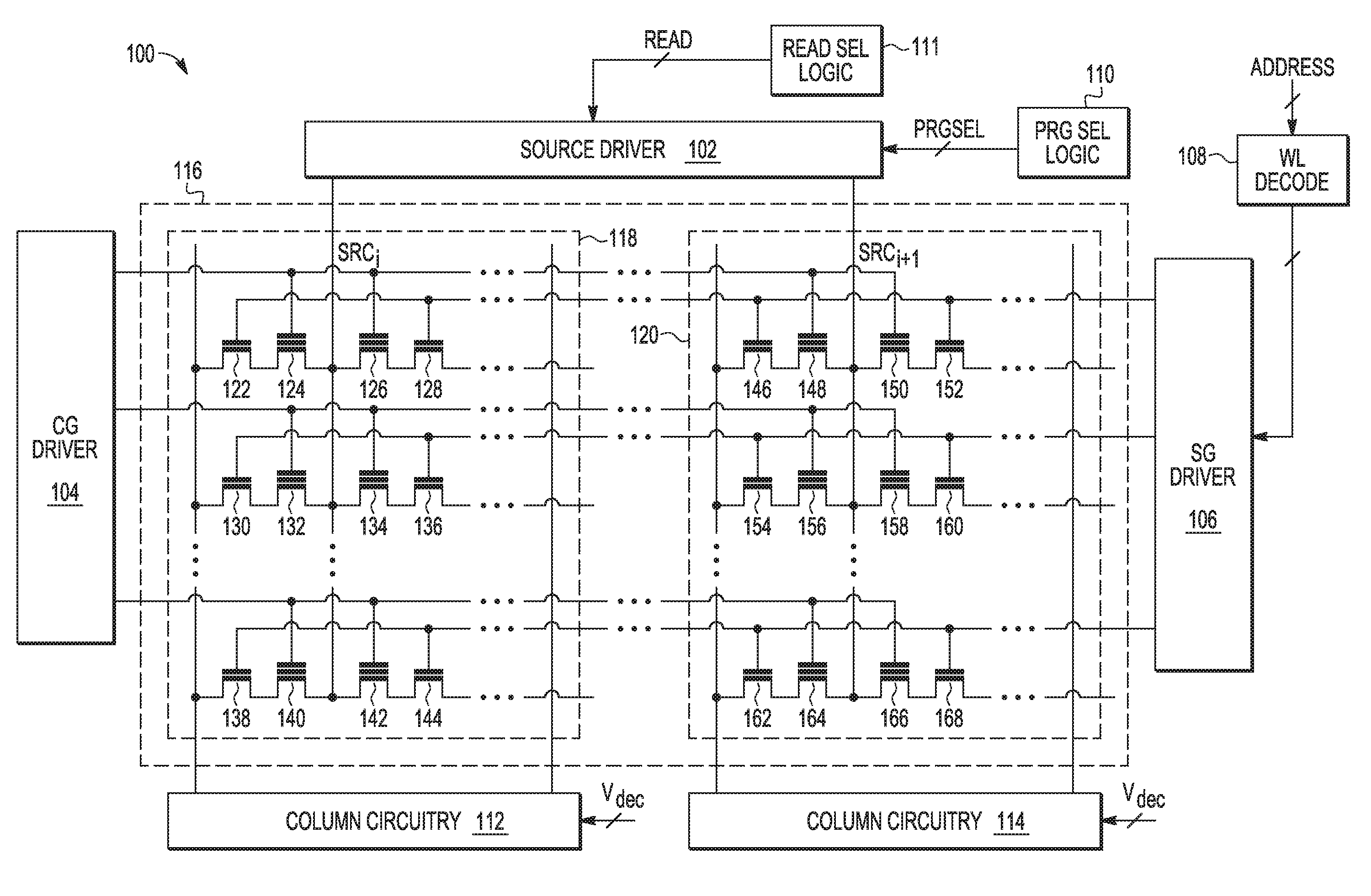
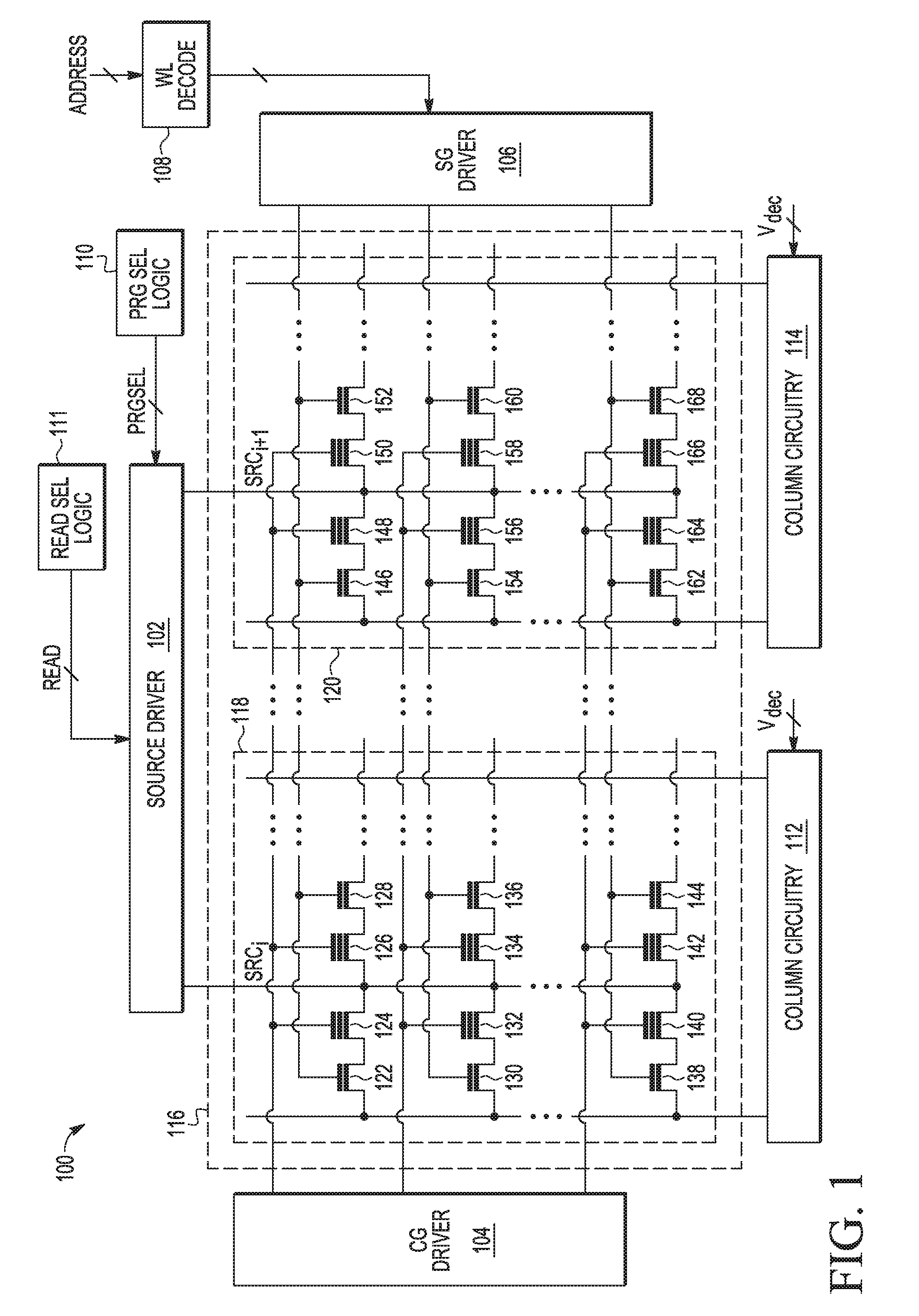
[0008]In certain memory circuit architectures, split gates may be employed. With some split-gate architectures, there may be a disadvantage of applying relatively high voltage levels to memory cells that may not be part of a current memory operation. For example, depending on the memory operation, voltages ranging from 0-9 V may be applied. This may be desirable for the memory cells subject to the operation, but may lead to undesirable levels of disturb for those memory cells that are not immediately subject to the operation. One potential solution to this problem may be to re-engineer a top dielectric layer of the split-gate cells to reduce the level of disturb. However, this may be difficult to achieve and / or increase manufacturing costs.

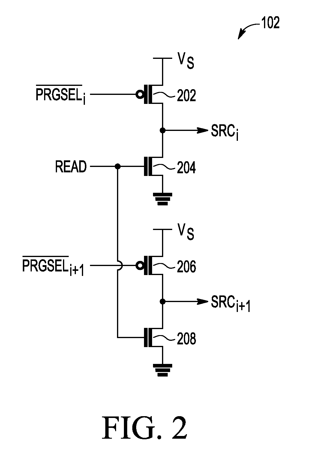
[0009]In some embodiments of the present disclosure, gate disturb may be reduced without having to re-engineer the dielectric layer(s). In some embodiments, unselected sources (e.g., sources of memory cells not immediately subject to a memory oper...


PUM


Abstract

A memory circuit has control gate circuitry (104) and select gate circuitry (106). A first memory cell (122 / 124) has a control gate coupled to the control gate circuitry, a select gate coupled to the select gate circuitry, a drain that is coupled to a first bit line for reading a logic state of the of the first memory cell, and a source. A second memory cell (150 / 152 or 158 / 160) having a control gate coupled to the control gate circuitry, a select gate coupled to the select gate circuitry, a drain that is coupled to a second bit line for reading a logic state of the of the second memory cell, and a source. A source control circuit (102) that, during programming of the first memory cell, outputs a first voltage to the source of the first memory cell and keeps the source of the second memory cell floating.

Description

BACKGROUND[0001]1. Field[0002]This disclosure relates generally to split-gate flash cell arrays, and more specifically, to systems and methods to mitigate program gate disturb in split-gate flash cell arrays.[0003]2. Related Art[0004]Within a split gate memory cell array, each row of memory cells may be coupled to a control gate driver which drives a required voltage level onto the control gates of the split gate memory cells in accordance with the desired operation. For example, the voltage applied to the control gate of a memory cell depends on whether the desired operation of that memory cell is a program select operation, a program deselect operation, an erase operation, an erase verify operation, a program verify operation, etc. However, this may result in high voltages being applied to other control gates within the array even when the particular memory cell is not the subject of the instant operation. Therefore, a need exists for systems and methods to mitigate program gate d...

Claims


Application Information

Patent Timeline
Patent Type & Authority Patents(United States)
IPC IPC(8): G11C16/34G11C16/10G11C16/26G11C16/30
CPCG11C16/3427G11C16/10G11C16/26G11C16/30G11C16/0425G11C16/24
Inventor ROY, ANIRBAN
Owner NXP USA INC
Why Eureka
Try Eureka