Touch panel and touch device with the same

a touch panel and touch technology, applied in the field of touch panel and touch device with the same, can solve the problems of high cost, easy physical damage, deterioration of the characteristic of the electrode part, etc., and achieve the effect of improving printing quality, reducing resistance of the touch panel, and high-quality touch panel

Active Publication Date: 2016-11-08
LG INNOTEK CO LTD
View PDF6 Cites 0 Cited by
  • Summary
  • Abstract
  • Description
  • Claims
  • Application Information

AI Technical Summary

Benefits of technology

[0006]The embodiment provides a touch panel representing improved reliability and a touch device with the same.
[0008]A sensing electrode of the touch panel according to the embodiment has a conductive pattern so that the pattern of the sensing electrode may be hidden in the active area. That is, the pattern may not be viewed even if the sensing electrode is made from a metal. In addition, even when the sensing electrode is applied to a large-size touch panel, the resistance of the touch panel can be reduced. In addition, even when the sensing electrode is formed through the printing process, the printing quality can be improved so that the high-quality touch panel can be ensured.
[0009]Further, the sensing electrode may include the first buffer layer disposed on the electrode layer, and the first buffer layer can prevent the electrode layer from being over-etched. Accordingly, the thickness of the electrode layer may be ensured so that electric characteristics can be improved. That is, during an etching process, the resistance increase caused by the reduction of the thickness of the electrode layer can be prevented.
[0010]Moreover, the sensing electrode may include a second buffer layer disposed under the electrode layer, and the second buffer layer can ensure the adhesive strength of the electrode layer. The electrode layer can be prevented from being delaminated due to the second buffer layer.
[0011]In addition, according to another embodiment, a top surface of the first buffer layer has an area wider than an area of a top surface of the sensing electrode. Due to the first buffer layer, the increase of visibility due to light reflected from the sensing electrode including the metallic material can be prevented. Particularly, the first buffer layer can reduce reflectivity of a lateral side of the sensing electrode as well as the top surface of the sensing electrode so that the touch panel is advantageous in terms of visibility. In addition, the visibility can be improved even at a wide viewing angle. Therefore, optical characteristics of the sensing electrode can be improved.

Problems solved by technology

Indium tin oxide (ITO), which has been most extensively used as a transparent electrode of the touch panel, has high cost and is easily subject to physical damage due to the bending or the flection of a substrate, so that the characteristic of the ITO for the electrode part is deteriorated.
Accordingly, the ITO is not suitable for a flexible device.
Further, when the ITO is applied to a touch panel having a large size, a problem occurs due to high resistance.

Method used


Image

  • Touch panel and touch device with the same
  • Touch panel and touch device with the same
  • Touch panel and touch device with the same

Examples


Embodiment Construction

[0031]In the following description of the embodiments, it will be understood that, when a layer (or film), a region, a pattern, or a structure is referred to as being “on” or “under” another substrate, another layer (or film), another region, another pad, or another pattern, it can be “directly” or “indirectly” on the other substrate, layer (or film), region, pad, or pattern, or one or more intervening layers may also be present. Such a position of the layer has been described with reference to the drawings.

[0032]The thickness and size of each layer shown in the drawings may be exaggerated, omitted or schematically drawn for the purpose of convenience or clarity. In addition, the size of elements does not utterly reflect an actual size.

[0033]Hereinafter, the embodiments will be described in detail with reference to the accompanying drawings.

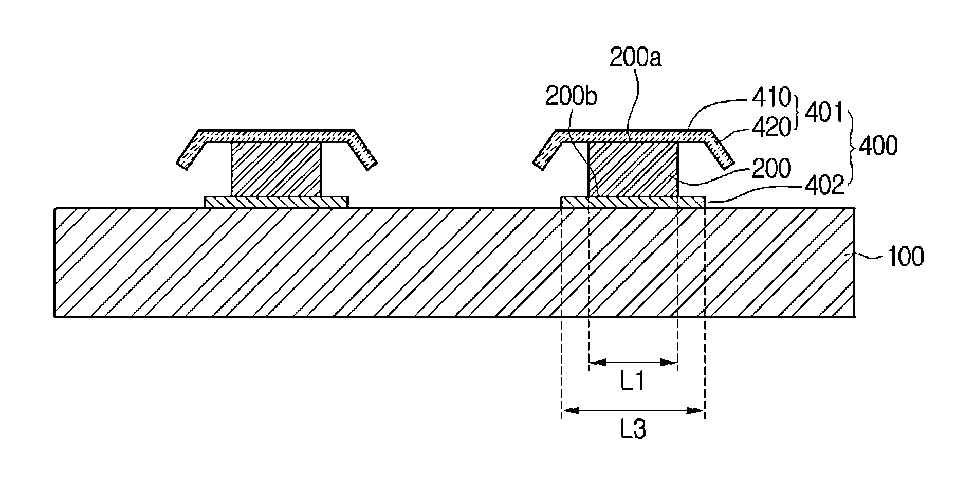
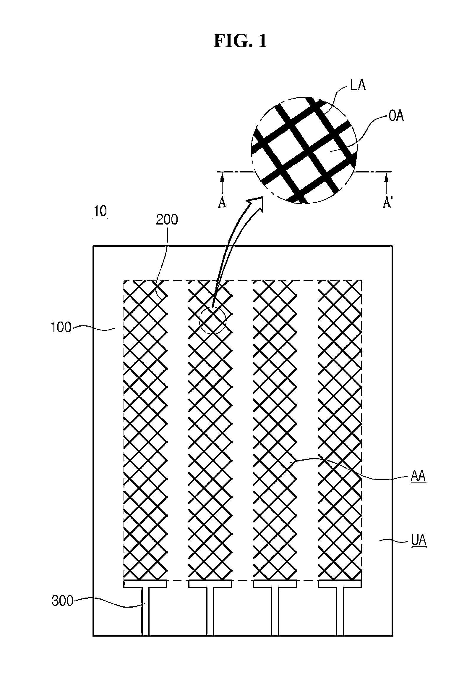
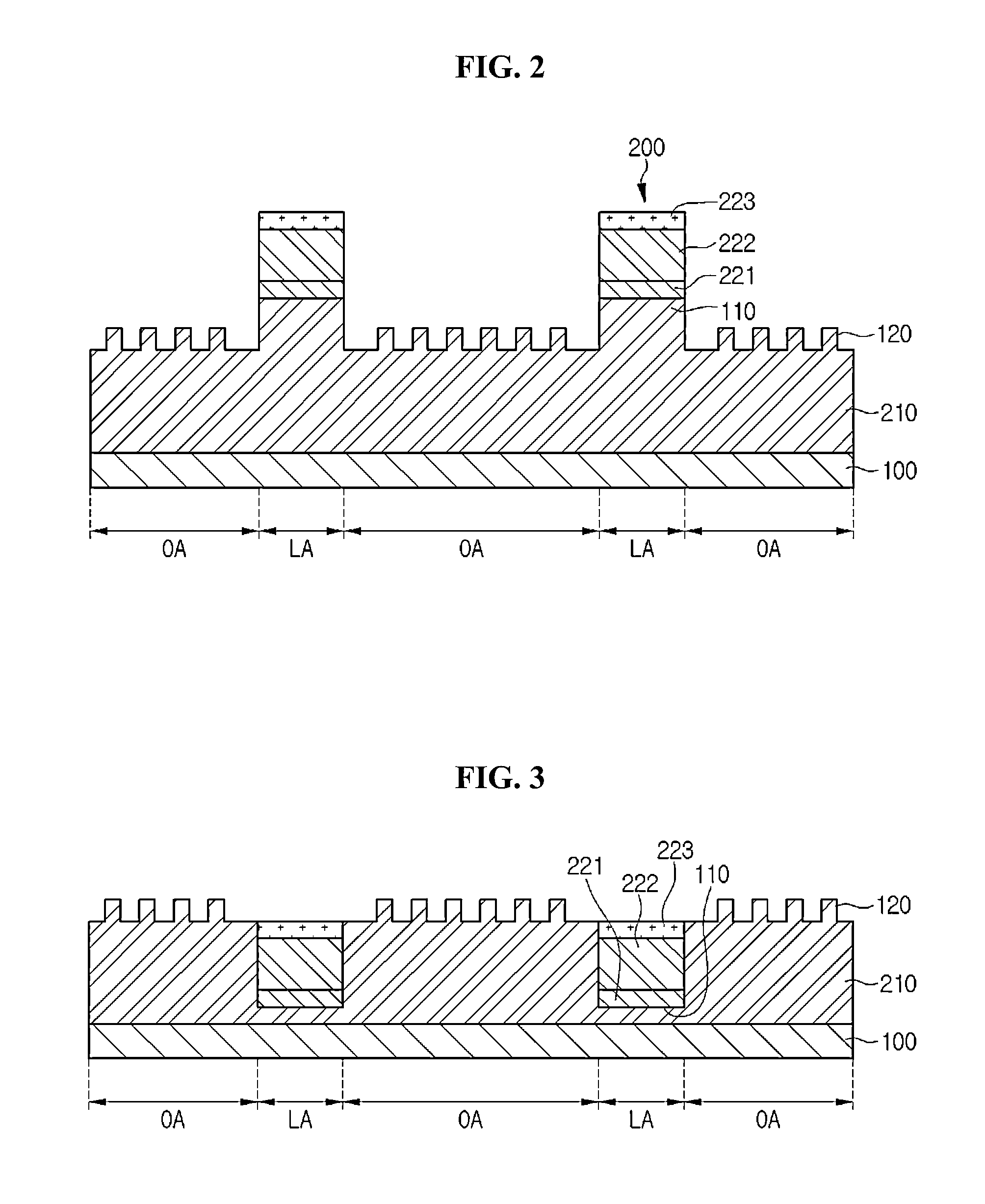
[0034]First, the touch window according to the embodiment will be described in detail with reference to FIGS. 1 and 2. FIG. 1 is a plan view sho...


PUM


Abstract

A touch panel includes a substrate; and a sensing electrode with a conductive pattern on the substrate, wherein the sensing electrode includes: an electrode layer; and a first buffer layer on the electrode layer.

Description

CROSS-REFERENCE TO RELATED APPLICATIONS[0001]This application claims the benefit under 35 U.S.C. §119 of Korean Patent Application Nos. 10-2013-0032090, filed Mar. 26, 2013, 10-2013-0070527, filed Jun. 19, 2013, and 10-2013-0089658, filed Jul. 29, 2013 which are hereby incorporated by reference in their entirety.BACKGROUND[0002]The embodiment relates to a touch panel and a touch device with the same.[0003]Recently, a touch panel, which performs an input function through the touch of an image displayed on a touch device by an input device such as a stylus pen or a hand, has been applied to various electronic appliances.[0004]The touch panel may be mainly classified into a resistive touch panel and a capacitive touch panel. In the resistive touch panel, the position of the touch point is detected by detecting the variation of resistance according to the connection between electrodes when pressure is applied to an input device. In the capacitive touch panel, the position of the touch p...

Claims


Application Information

Patent Timeline
Patent Type & Authority Patents(United States)
IPC IPC(8): G06F3/046G06F3/044
CPCG06F3/046G06F3/044G06F2203/04103G06F3/0443
Inventor LEE, DONG KEONKIM, HYUN SOOSHIN, JUN SIKYANG, JOON HYUKBANG, JUNG HWANKOO, CHAN KYU
Owner LG INNOTEK CO LTD
Why Eureka
Try Eureka