Planar sensor and its manufacturing method
a sensor and planar technology, applied in the field of planar sensors, can solve the problems of time-consuming and complex separation of sensor and flooring, complex contact arrangement between sensor conductors and connection cables, etc., and achieve the effect of facilitating the manufacturing process
- Summary
- Abstract
- Description
- Claims
- Application Information
AI Technical Summary
Benefits of technology
Problems solved by technology
Method used
Image

Examples
Embodiment Construction
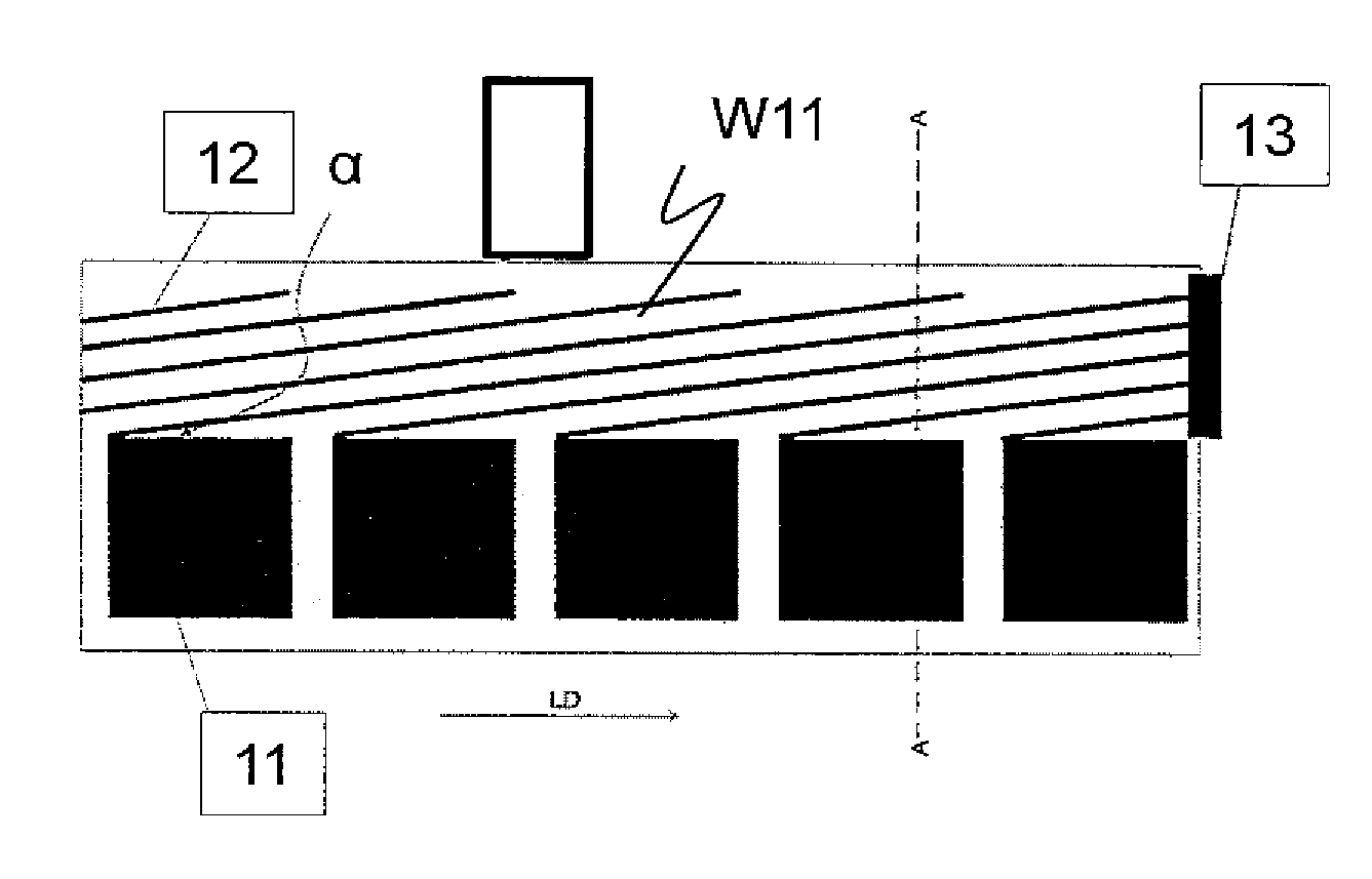
[0029]The present invention is based on an idea to integrate a planar sensor and a flooring into a unitary floor sensor structure and to manufacture this unitary structure in a continuous manufacturing process. The planar sensor is thin and has a thickness 10-100 μm whereby the flooring is essentially thicker and has a thickness 1-10 mm. Further, the flooring layer is provided with peeling areas or peeling stripes.
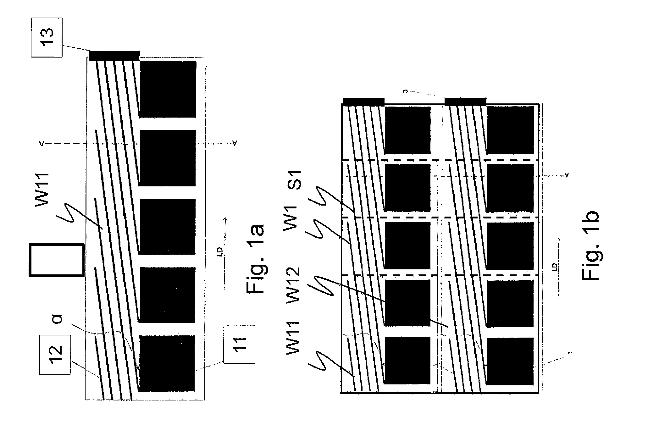
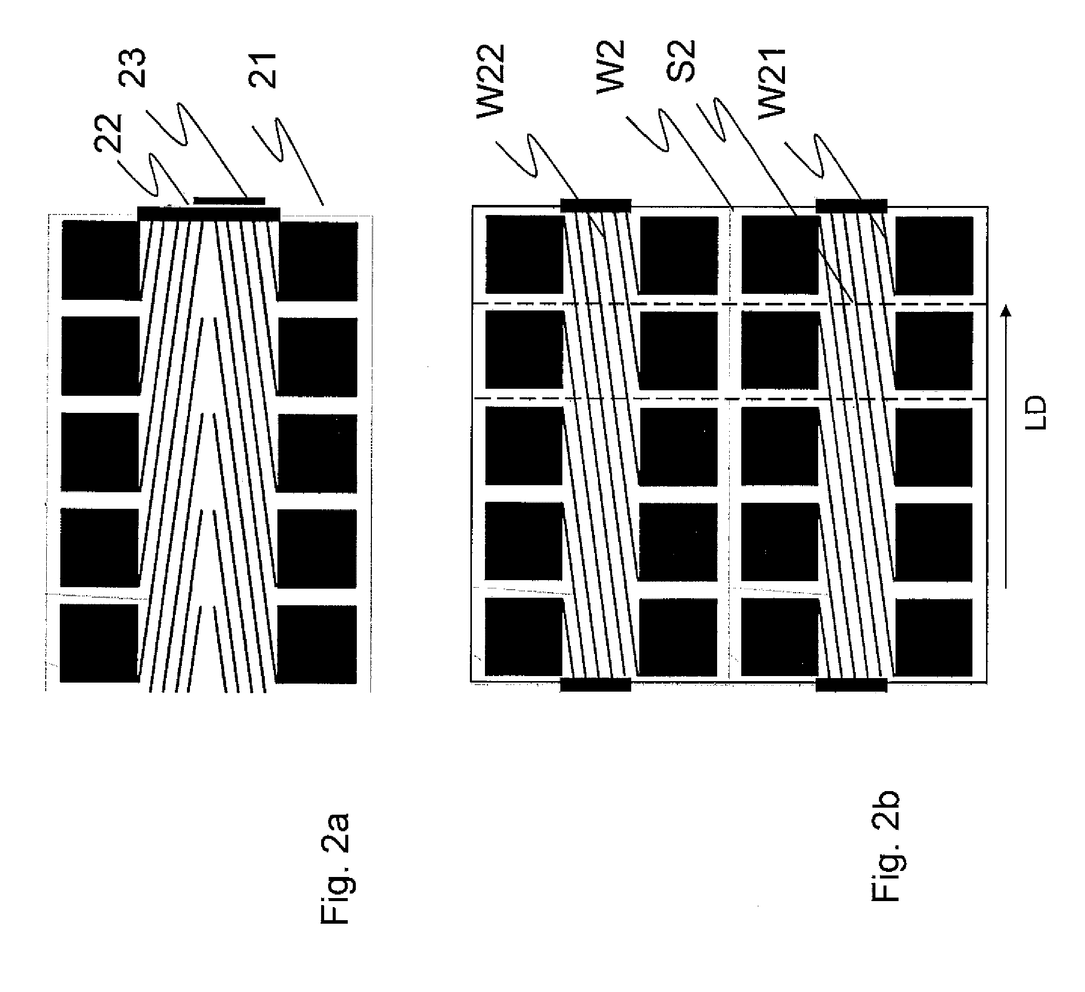
[0030]FIG. 1b illustrates a floor sensor W1 for monitoring electrically conductive objects, for example the movement and location of a human on a floor. The sensor web W1 comprises several, in FIG. 1b two, identical parallel sensor web units W11, W12 having successive electrically conductive areas 11 according to FIG. 1a. A conductor 12 connects the electrically conductive area 11 to an output 13. The output 13 is provided with a connector. The parallel conductors 12 extend linearly and form an angle α to the longitudinal direction LD of the web.
[0031]The sensor web W1 is ...
PUM
| Property | Measurement | Unit |
|---|---|---|
| thickness | aaaaa | aaaaa |
| thickness | aaaaa | aaaaa |
| thickness | aaaaa | aaaaa |
Abstract
Description
Claims
Application Information
PatSnap Eureka turns technology decisions into work you can execute. Powered by our Innovation Knowledge Graph, it runs expert workflows across engineering, life sciences, materials and intellectual property. Get your review-ready output in minutes.


